關鍵詞: DVGA , LMH6522 , NS , 數控可編增益
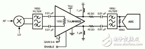
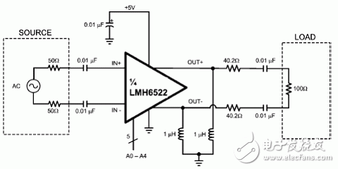
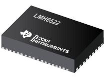
NS公司的LMH6522是高性能四路數控可編增益(DVGA)放大器,-3dB帶寬1400MHz,電壓26dB,增益可編1dB/步,200MHz的OIP3為49dBm,噪音為8.5dB,可進行并聯和串聯增益控制,主要用在蜂窩基站,寬帶和窄帶IF取樣接收器,寬帶直接變換和ADC驅動器.本文介紹了LMH6522主要特性,方框圖, 基本連接電路圖, 典型應用電路圖以及LMH6522EVAL評估板輸入和輸出電路, 邏輯插頭電路圖, 信號通路電路和評估板元件布局圖.
2011-8-26 12:57:35 上傳
The LMH6522 contains four, high performance, digitally controlled variable gain amplifiers (DVGA). It has been designed for use in narrowband and broadband IF sampling applications.
Typically, the LMH6522 drives a high performance ADC in a broad range of mixed signal and digital communication applications such as mobile radio and cellular base stations where automatic gain control (AGC) is required to increase system dynamic range.
Each channel of LMH6522 has an independent, digitally controlled attenuator and a high linearity, differential output, amplifier.
All circuitry has been optimized for low distortion and maximum system design flexibility. Power consumption is managed by a three-state enable pin. Individual channels can be disabled or placed into a Low Power Mode or a higher performance, High Power Mode.
The LMH6522 digitally controlled attenuator provides precise 1dB gain steps over a 31dB range. The digital attenuator can be controlled by either a SPI™ Serial bus or a high speed parallel bus.
The output amplifier has a differential output, allowing large signal swings on a single 5V supply. The low impedance output provides maximum flexibility when driving a wide range filter designs or analog to digital converters. For applications which have very large changes in signal level LMH6522 can support up to 62dB of gain range by cascading channels.
The LMH6522 operates over the industrial temperature range of −40°C to +85°C. The LMH6522 is available in a 54-Pin, thermally enhanced, LLP package.
LMH6522主要特性:
■ OIP3: 49dBm @ 200MHz
■ Noise Figure: 8.5dB
■ Voltage Gain: 26dB
■ 1dB Gain Steps
■ −3dB bandwidth of 1400 MHz
■ Gain Step Accuracy: 0.2 dB
■ Disable function for each channel
■ Parallel and Serial gain control
■ Low Power Mode for power management flexibility
■ Small footprint LLP package
LMH6522應用:
■ Cellular base stations
■ Wideband and narrowband IF sampling receivers
■ Wideband direct conversion
■ ADC Driver
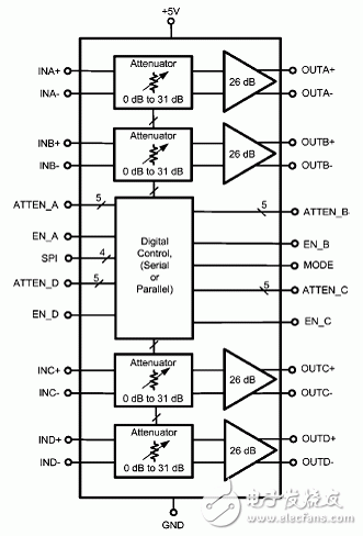
圖1. LMH6522方框圖
2011-8-26 12:57:35 上傳
下載附件 (12.04 KB)圖2. LMH6522基本連接電路圖
2011-8-26 12:57:35 上傳
下載附件 (16.31 KB)圖3. LMH6522典型應用電路圖
LMH6522EVAL評估板
The LMH6522EVAL evaluation board is designed to aid in the characterization of National Semiconductor’s High Speed LMH6522 Digital Controlled Variable Gain Amplifier (DVGA). Use the evaluation board as a guide for high frequency layout and as a tool to aid in device testing and characterization.
The LMH6522 DVGA has differential inputs and differential outputs. The evaluation board has been designed to easily interface with 50Ω single ended test equipment. The LMH6522EVAL evaluation board is shipped with input and output transformers installed to convert the DVGA differential inputs and outputs to single ended signal paths. As built, the signal path uses the IN+ and OUT− marked connectors. The IN− and OUT+ signal paths are grounded. The signal paths are fully symmetrical.
To preserve proper bias voltages there are DC blocking capacitors on both the input and output signal traces. The input pins of the LMH6522 will self bias to approximately mid supply (2.5V). The output pins need to be biased to near ground potential.
Inductors are installed on the evaluation board to provide proper output biasing. The bias current is approximately 36 mA per output pin. Capacitors between the amplifier and the output transformer will prevent offset currents from flowing through the transformer primary coil. Many transformers will show increased distortion products when there is a DC current flowing through the primary coil.
Transformers TINA– TIND can provide both impedance matching as well as single ended to differential conversion.
The board is shipped with 2:1 impedance ratio transformers (1.4:1 Voltage ratio) that will match 50Ω equipment with the 100Ω input impedance of the LMH6522 DVGA .
On the output side of the board are transformers TOUTA - TOUTD. The output transformers were chosen to provide a good compromise between distortion performance and physical size. The LMH6522 is capable of driving a wide range of load impedances. A 200 Ohm load impedance was chosen for the evaluation board to emulate performance with a 100 Ohm back terminated filter. Other configurations are possible with minor rework of the evaluation board.
Capacitors CCOA+/− through CCOD+/− are installed to isolate the DVGA outputs from the output transformer primary windings. The output resistors are 40.2 Ohm matching resistors.
The output impedance of the LMH6522 amplifier is very low (10Ω @ 50MHz), and the 40.2 Ohm resistors provide termination for the 100 Ohm load presented by the transformer when the evaluation board is connected to 50 Ohm test equipment.
The JTX–2–10T output transformers have a 1:2 impedance ratio.
The LMH6522 DVGA is configured to have a maximum gain of 26dB. The transformers and matching resistors contribute a loss of approximately 7.5 dB. Gain through the board should measure approximately 18.6 dB.
2011-8-26 12:57:35 上傳
下載附件 (189.19 KB) 電子發燒友App






評論