Variable Voltage Supply Design
In this example application, the DS1809 is used to control the voltage output of an LP2951 voltage regulator. The intent is to create a variable power supply that has precise voltage control and defined voltage limits. This circuit can be powered by many sources including wall socket adapters and batteries, which provide portability for the supply circuit.The circuit in Figure 1 shows how the output of the LP2951 is controlled by the DS1809. Any low-output noise voltage regulator will do. The DS1809 is a pushbutton controlled, 64 position digital potentiometer. It is available in 10kΩ, 50kΩ, and 100kΩ sizes. The voltage divider circuit composed of R1, R2, and the DS1809 adjusts the voltage seen on the Feedback pin (pin 7) of the LP2951. By changing the potential here, the output voltage of the LP2951 is adjusted.
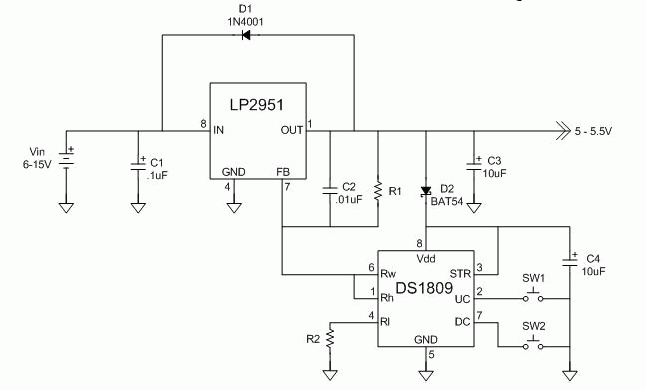
Figure 1. Variable Power Supply Circuit, 5.0V To 5.5V Range
C1 is a decoupling capacitor used to provide voltage stability for the input. C2 is a bypass capacitor used to reduce AC noise on the output voltage signal. C3 is used to provide voltage stability when a load is present on the output of the regulator. C4 is a decoupling capacitor for the DS1809. D1 is used to protect the LP2951 from damage when C2 is fully charged and the input is disconnected. D2 and C4 are needed to allow the DS1809 to auto-store the wiper position when the circuit powers down. The Rh terminal of the DS1809 is connected to the wiper terminal Rw to minimize noise.
R1, R2, and the size of the digital potentiometer are used to determine the maximum and minimum voltage range of output voltage signal. Equation 1 shows the formula that is used to select the sizes of R1, R2, and the DS1809.
Equation 1. VOUT Formula.

VOUT is the voltage seen on the output pin of the LP2951, and VREF is the internal reference comparator voltage seem the FeedBack pin (pin 7), and is typically 1.235V. The current through R2 and the DS1809 is the same current seen through R1. This current is calculated by dividing the reference voltage by the combined resistance of R2 and the DS1809. The voltage seen on the output pin is this current times the sum of R1, R2, and the resistance seen through the DS1809.
The first step is to determine the voltage range the circuit will supply. We can design a supply for a range of 5.0V to 5.5V. This was done by substituting 5.0V and 5.5V for VOUT and 1.235V for VREF into Equation 1. The result will look like the formulas in Equation 2.
Equation 2. VOUT Calculation for 5.0V to 5.5V range.
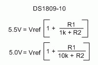
From the data sheet of the DS1809, we use the maximum wiper resistance value and R2 to determine R1 for the maximum voltage value. We use the maximum resistance of the DS1809 and R2 to calculate R1 for the minimum value of the voltage supply. We solve the two equations for R1, then substitute and solve for R2. Using the above equations, we get 66.75kΩ for R2 and 233.90kΩ for R1. Using a 68kΩ 1/8 watt resistor and a 220kΩ 1/8 watt resistor, we get the circuit in Figure 1. The .5V range divided by the 64 positions provided by the DS1809 gives us 7.8mV/step from 5.0V to 5.5V.
To use a broader range, from 4.5V to 5.5V, simply use the same equations substituting in the desired voltage ranges.
Equation 3. VOUT Calculation for 4.5V to 5.5V range.
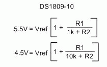
Using these equations, we find using a 10kΩ DS1809 that R1 is 101.4kΩ and R2 is 28.3kΩ. We get a 15.6mV/step accuracy using this 1V range.
Equation 4. VOUT Calculation for 3.0V to 5.5V range.
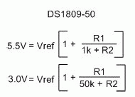
Using the above equation, we choose the 50kΩ pot for a wider voltage range. We determine that R1 is 119.5kΩ and R2 is 33.6kΩ. The 2.5V range allows for 39mV/step accuracy.
Current Limitations
The maximum current that can be drawn from the LP2951 is 100mA. For stable functionality, the maximum current that can flow through the resistive elements of the DS1809 is 4mA. In this circuit, the current drawn through the DS1809 wiper is 32μA and the current into the VCC pin of the DS1809 115μA in standby, and 350μA when actively adjusting the wiper positions. The LP2951 Feedback pin (pin 2) is internally connected to an amplifier that compares the voltage from the R1/(R2+R1) voltage divider to the internal reference voltage of 1.235V. Typical current drawn from the Feedback pin is 20nA.Summary
This supply design is portable and easy to build. It allows precise control over a variety of voltage ranges. More precise control (7.8mV/step) is achieved when using a small (0.5V) voltage range. Less precise control (39.0mV/step) is possible when using a larger (2.5V) voltage range. The pushbutton interface of the DS1809 lets single step adjustments to be made to the output voltage. If desired, the wiper can be shifted continuously by pressing and holding either pushbutton. After an initial 0.5 second delay, the wiper will automatically step in the desired direction once every 100 milliseconds until the end-position is reached.Other digital potentiometers can be used, such as the DS1804, which uses 3-wire communication, or a DS1803, which uses 2-wire communication to adjust the wiper position. Thus, it is possible to use a microprocessor to control the output voltage of this circuit.
The DS1809 will not increment or decrement the wiper position past the digital potentiometer’s endpositions, and will not auto-step unless either pushbutton is depressed for more than 0.5 seconds. This means that the voltage will never exceed the maximum and minimum values designed into the circuit. Pressing the SW1 pushbutton decrements the output voltage. Similarly, SW2 increments the output voltage by the same amount per press. Therefore, even if SW1 or SW2 pushbuttons are inadvertently pressed, the output voltage changes very little and is never allowed to exceed the set range limits.
Use of a DS1809 digital potentiometer allowed convenient manual control of a voltage regulator. The circuit was built on a breadboard with a 9V battery supply and alternatively, a 20V power supply. Because the standby current of the LP2951 is only 60μA and the low level of standby current drawn by the circuit as a whole, a 9V battery can be used for a power source. This makes the circuit small and portable. The fixed voltage range of this supply prevents accidental over-voltage of the ICs.
 電子發(fā)燒友App





評(píng)論