Abstract: The MAX1463 is a highly integrated, low power, two-channel sensor signal processor optimized for industrial and process control applications such as pressure sensing, RTD and thermal-couple linearization, weight sensing, and remote process monitoring with limit indication. The MAX1463 accommodates sensors with outputs ranging from 1mV/V to 1V/V. It includes two 16-bit output DACs, two 12-bit PWM outputs, and supports 4-20mA output. It incorporates a 16-bit CPU, 4K bytes of program and 128 bytes of user flash memory.
The MAX1463 includes an internal temperature sensor that can be used for correction of temperature dependent signals or as a stand-alone thermometer. For applications where the supply voltage, VDD, can not be held constant, the supply rejection performance of the temperature sensor readings may not be adequate and the readings should be corrected for supply variations. This document describes the procedure to correct for the supply rejection error of the internal temperature sensor readings in the MAX1463.
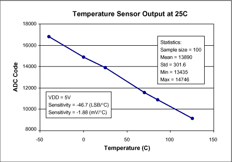
Figure 1. Typical temperature sensor output as a function of temperature.
In situations where the ADC reference voltage, ADCref, is fixed but VDD voltage is allowed to change, any ADC reading will include an error that is a function of VDD and the ADC offset. The output of the ADC (as a fraction of its reference voltage) includes the ADC offset that is proportional to the ADC reference voltage. In applications where the ADC's input voltage is ratiometric to VDD and VDD is selected as ADCref, the ADC output will be ratiometric to VDD.
In the MAX1463, when performing temperature conversion, the internal bandgap voltage, VBG = 1.25V, is automatically selected as ADCref. Therefore, the ADCref is always fixed when temperature conversion is performed. Hence, any deviation of the VDD voltage from its target value will cause significant supply rejection error in ADC output code (Figure 2, Figure 3). Situations related to VDD control and ADCref selections and supply rejection capability of the MAX1463 can be divided in three categories: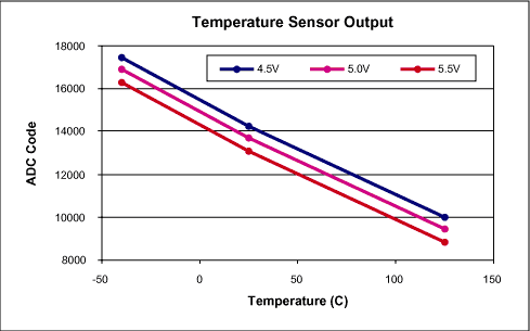
Figure 2. Typical temperature sensor output as a function of temperature and supply voltage.
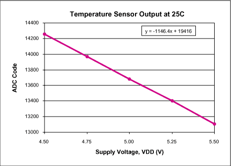
Figure 3. Typical temperature sensor output as a function of supply voltage.
To determine the correction factor, a simple procedure must be performed prior to temperature compensation. This procedure need to be performed only one time and it can be done at any temperature since the effect of temperature on the supply rejection of the ADC conversions is relatively small, Figure 4. For very high accuracy applications, it may be required to perform this procedure at every temperature. The procedure for determining correction factor for the ADC supply rejection error must yield the slope of the ADC code as a function of VDD at a constant temperature.
It is extremely important that the device temperature remains unchanged during this procedure.
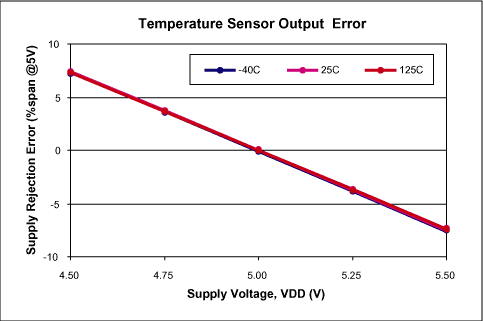
Figure 4. Typical temperature sensor conversion error as a function of supply voltage and temperature.
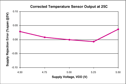
Figure 5. Typical temperature sensor output after correction for conversion error has been applied.
The overhead caused by the requirement to perform supply rejection correction to the ADC output is approximately 18usec that accounts for two additional subtractions and one additional multiplication operation in for every temperature reading. Also, because temperature change is normally very slow compared to input signal changes and very fast CPU cycles, in most applications it is sufficient to read the temperature one time for every 100 times of input signal conversions. Therefore, the overhead will account for insignificant portion of the overall cycle time.
The MAX1463 includes an internal temperature sensor that can be used for correction of temperature dependent signals or as a stand-alone thermometer. For applications where the supply voltage, VDD, can not be held constant, the supply rejection performance of the temperature sensor readings may not be adequate and the readings should be corrected for supply variations. This document describes the procedure to correct for the supply rejection error of the internal temperature sensor readings in the MAX1463.
Description
The MAX1463 includes an ADC that is used to convert various analog inputs to digital codes. The ADC uses the internal 1.25V band-gap reference (VBG) when converting the temperature sensor's output. For any other conversion, the ADC reference can be selected as VDD for conversions ratiometric to the power supply, voltage on the VREF pin for conversions relative to an external voltage, or VBGx4 which is an internally generated "pseudo" 5.0 volt reference source.
Figure 1. Typical temperature sensor output as a function of temperature.
In situations where the ADC reference voltage, ADCref, is fixed but VDD voltage is allowed to change, any ADC reading will include an error that is a function of VDD and the ADC offset. The output of the ADC (as a fraction of its reference voltage) includes the ADC offset that is proportional to the ADC reference voltage. In applications where the ADC's input voltage is ratiometric to VDD and VDD is selected as ADCref, the ADC output will be ratiometric to VDD.
In the MAX1463, when performing temperature conversion, the internal bandgap voltage, VBG = 1.25V, is automatically selected as ADCref. Therefore, the ADCref is always fixed when temperature conversion is performed. Hence, any deviation of the VDD voltage from its target value will cause significant supply rejection error in ADC output code (Figure 2, Figure 3). Situations related to VDD control and ADCref selections and supply rejection capability of the MAX1463 can be divided in three categories:
-
VDD = constant, ADCref = constant (internal or external)
Best situation. No supply rejection correction is required to neither of the temperature nor input signal conversions. -
VDD = not constant, ADCref = VDD.
- No supply rejection correction is required to the input signal conversions since the ADC reference voltage moves with VDD and any contribution of the ADC offset will be scaled accordingly.
- However, supply rejection correction must be applied on the temperature sensor conversions. This is because the fixed VBG voltage is internally selected as ADCref.
-
VDD = not constant, ADCref = constant (internal or external)
Supply rejection correction must be applied to all ADC conversions regardless of the source of input.

Figure 2. Typical temperature sensor output as a function of temperature and supply voltage.

Figure 3. Typical temperature sensor output as a function of supply voltage.
Correcting for the VDD Variations
The procedure described below is for applications where the MAX1463 have been configured for ADCref = VDD and VDD is expected to change. In this case, correction have to be applied every time a temperature sensor reading is performed. The correction to be applied is referenced to a target voltage, VDDtarget that is decided at the time of compensation. VDDtarget is typically 5V.To determine the correction factor, a simple procedure must be performed prior to temperature compensation. This procedure need to be performed only one time and it can be done at any temperature since the effect of temperature on the supply rejection of the ADC conversions is relatively small, Figure 4. For very high accuracy applications, it may be required to perform this procedure at every temperature. The procedure for determining correction factor for the ADC supply rejection error must yield the slope of the ADC code as a function of VDD at a constant temperature.
It is extremely important that the device temperature remains unchanged during this procedure.

Figure 4. Typical temperature sensor conversion error as a function of supply voltage and temperature.
Determining the Correction Factor
- Select VDD as reference voltage for the ADC.
- Set VDD to the target voltage at which it is expected to be operated. Target voltage is typically 5V.
- Initiate ADC conversion of VDD.
- Read ADC code for VDD, VDDtarget.
- Set VDD = 4.5V.
- Initiate ADC conversion of VDD.
- Read ADC code for VDD, VDD4.5.
- Initiate ADC conversion of the temperature sensor.
- Read ADC code for temperature sensor output, ADC4.5.
- Set VDD = 5.5V.
- Initiate ADC conversion of VDD.
- Read ADC code for VDD, VDD5.5.
- Initiate ADC conversion of the temperature sensor.
- Read ADC code for temperature sensor output, ADC5.5.
-
Calculate the ADCslope:
ADCslope = (ADC5.5 - ADC4.5) / (VDD5.5 - VDD4.5) [code/Volt]
- The ADCslope and VDDtarget values should be used in the compensation algorithm for correcting all future temperature sensor readings.
Applying Correction for VDD Variations
During normal operation of the signal conditioner, the correction formula has to be applied every time a temperature sensor reading is performed.- Select temperature sensor output to be input of the ADC.
- Perform an ADC reading, ADCmeas.
- Select VDD to be input of the ADC.
- Perform a VDD reading, VDDmeas.
-
Apply correction formula:
ADCcorrected = ADCmeas + (ADCslope × (VDDtarget - VDDmeas))

Figure 5. Typical temperature sensor output after correction for conversion error has been applied.
The overhead caused by the requirement to perform supply rejection correction to the ADC output is approximately 18usec that accounts for two additional subtractions and one additional multiplication operation in for every temperature reading. Also, because temperature change is normally very slow compared to input signal changes and very fast CPU cycles, in most applications it is sufficient to read the temperature one time for every 100 times of input signal conversions. Therefore, the overhead will account for insignificant portion of the overall cycle time.
 電子發燒友App









評論