光學特性
輸入發光二極管:通常采用高效的砷化鎵(GaAs)或磷化銦(InP)等材料制成,其正向電壓一般在 1.2V 到 1.5V 之間,正向電流典型值約為 5mA 到 20mA,能夠在較低的電流下產生足夠強度的光信號,確保光耦的正常工作和信號傳輸。
輸出光電探測器:與輸入發光二極管光學耦合,具有較高的光電轉換效率,可將接收到的光信號快速、準確地轉換為電信號,其光譜響應范圍通常與輸入發光二極管的發光波長相匹配,以實現最佳的光電轉換效果。
Input light emitting diode: usually made of high-efficiency gallium arsenide (GaAs) or indium phosphide (InP) and other materials, its forward voltage is generally between 1.2V and 1.5V, and the typical forward current value is about 5mA to 20mA, which can generate sufficient intensity optical signal at a lower current to ensure the normal operation of the optocouple and signal transmission.
Output photodetector: optically coupled with the input light-emitting diode, with high photoelectric conversion efficiency, the received light signal can be quickly and accurately converted into an electrical signal, and its spectral response range is usually matched with the luminous wavelength of the input light-emitting diode to achieve the best photoelectric conversion effect.
電學特性
電流傳輸比:一般在 100% 到 500% 之間,較高的電流傳輸比意味著在輸入側給定一定電流時,輸出側能夠獲得相對較大的電流,從而可以更好地驅動后續電路,適用于需要較大驅動電流的負載。
輸入輸出電容:輸入輸出之間的電容一般在幾個皮法到幾十皮法之間,較低的電容值有助于減少信號傳輸過程中的延遲和失真,提高信號的傳輸速度和質量,特別是在高頻信號傳輸時更為重要。
集電極 - 發射極飽和電壓:當輸出晶體管處于飽和導通狀態時,集電極 - 發射極之間的飽和電壓通常在 0.2V 到 0.4V 左右,較低的飽和電壓可以降低輸出級的功耗,提高光耦的效率和可靠性。
Current transmission ratio: Generally between 100% and 500%, the higher current transmission ratio means that when the input side is given a certain current, the output side can obtain a relatively large current, so that the subsequent circuit can be better driven, suitable for the load that requires a larger drive current.
Input and output capacitance: The capacitance between the input and output is generally between several picomethods and dozens of picomethods, and the lower capacitance value helps to reduce the delay and distortion in the signal transmission process, improve the transmission speed and quality of the signal, especially when the high-frequency signal transmission is more important.
Collector-emitter saturation voltage: When the output transistor is in a saturated on-state, the saturation voltage between the collector-emitter is usually around 0.2V to 0.4V, and the lower saturation voltage can reduce the power consumption of the output stage and improve the efficiency and reliability of the optocoupler.
傳輸特性
傳輸速度:具有較高的傳輸速度,能夠滿足高速數字信號的傳輸需求,其傳播延遲時間一般在納秒級別,典型值約為 20ns 到 50ns 左右,可確保輸入信號和輸出信號之間的快速同步,減少信號傳輸延遲對系統性能的影響。
共模抑制比:較高,通常可達 10kV/μs 以上,能夠有效抑制共模信號的干擾,在存在共模噪聲的環境中,如工業現場的強電磁干擾或長距離傳輸線路中的共模干擾等,能保證信號的準確傳輸和系統的正常運行。
Transmission speed: It has a high transmission speed, which can meet the transmission needs of high-speed digital signals, and its propagation delay time is generally at the nanosecond level, with a typical value of about 20ns to 50ns, which can ensure the rapid synchronization between the input signal and the output signal, and reduce the impact of signal transmission delay on system performance.
Common mode rejection ratio: high, usually up to 10kV/μs or more, can effectively inhibit the interference of common mode signals, in the presence of common mode noise in the environment, such as strong electromagnetic interference in industrial sites or common mode interference in long-distance transmission lines, to ensure the accurate transmission of signals and the normal operation of the system.
隔離特性
隔離電壓:輸入和輸出之間的隔離電壓高達 3750V rms 或更高,具有出色的電氣隔離性能,能有效防止輸入側的高電壓、大電流等電氣干擾對輸出側電路的影響,保障系統的安全性和穩定性,適用于各種需要電氣隔離的場合,如工業自動化、電力電子設備、通信基站等。
絕緣電阻:通常在數千兆歐以上,高絕緣電阻可進一步減少漏電流,降低電氣干擾的可能性,確保隔離效果的可靠性。
Isolation voltage: The isolation voltage between the input and output is as high as 3750V rms or higher, with excellent electrical isolation performance, which can effectively prevent the input side of high voltage, high current and other electrical interference on the output side of the circuit, to ensure the safety and stability of the system, suitable for a variety of occasions requiring electrical isolation, such as industrial automation, power electronic equipment, communication base stations, etc.
Insulation resistance: usually above thousands of megohm, high insulation resistance can further reduce leakage current, reduce the possibility of electrical interference, and ensure the reliability of the isolation effect.
工作條件
工作溫度范圍:一般為 - 40℃到 + 125℃,寬溫度范圍使得該光耦能夠在惡劣的環境條件下穩定工作,無論是在高溫的工業現場還是在低溫的戶外設備中,都能保持良好的性能,可適應各種不同的工作環境,如汽車電子、航空航天、戶外通信基站等領域。
Operating temperature range: generally -40 ℃ to + 125℃, the wide temperature range makes the optocoupler can work stably under harsh environmental conditions, whether it is in the high temperature industrial site or in the low temperature outdoor equipment, can maintain good performance, can be adapted to a variety of different working environments, such as automotive electronics, aerospace, outdoor communication base stations and other fields.
電源電壓:輸入側和輸出側的電源電壓范圍較寬,輸入側一般可在 3V 到 5V 之間正常工作,輸出側可在 5V 到 15V 之間穩定運行,能夠與多種不同的電源系統兼容,方便在各種電路中進行應用和設計。
The input side and the output side of the power supply voltage range is wide, the input side can generally work between 3V and 5V, the output side can run stably between 5V and 15V, and can be compatible with a variety of different power systems, convenient for application and design in various circuits.
封裝特性
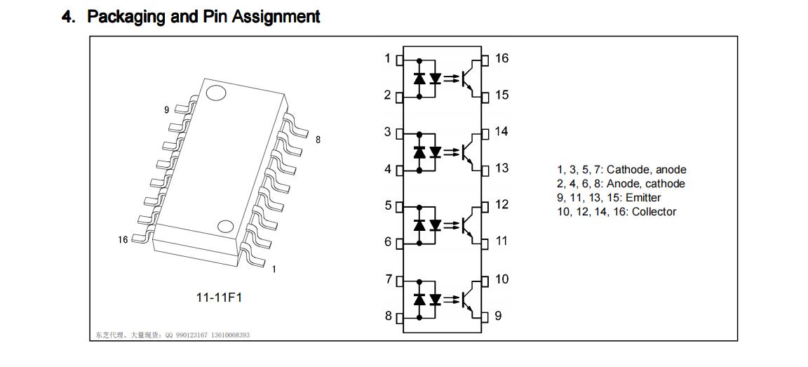
封裝形式:采用標準的 DIP、SOP 或 SMD 等封裝形式,具有良好的機械穩定性和電氣連接可靠性,易于焊接和安裝,可適應手工焊接和自動化貼片生產等多種生產工藝,在電路板上的布局也較為靈活,能夠滿足不同的電路設計需求。
引腳間距:引腳間距適中,通常為 2.54mm 或更小,有利于在高密度電路板上進行布局和布線,減少電路板的尺寸和成本。
Package form: The standard DIP, SOP or SMD package form, with good mechanical stability and electrical connection reliability, easy to weld and install, can adapt to manual welding and automatic patch production and other production processes, the layout on the circuit board is also more flexible, to meet different circuit design needs.
審核編輯 黃宇
-
光耦合器
+關注
關注
8文章
498瀏覽量
36259
發布評論請先 登錄
相關推薦
仙童FOD3150替代群芯微驅動光電耦合器型號QX3150美林美深
威世VOL3120替代群芯微驅動光電耦合器QX341美林美深
東芝TLP620替代群芯微驅動光電耦合器QX814美林美深
耦合器選型對設備效率的影響
耦合器的噪音控制技術 耦合器性能測試標準與方法
高性能光耦合器TLP2362:為您的工業與通信應用提供最佳選擇
TLP2301光電耦合器紅外LED和光電IC英文手冊
探索TLP2301:高效隔離的高速光耦合器
TOSHIBA東芝TLP2362光耦合器產品規格書
無線耦合器怎么安裝的
東芝光電耦合器IRED和光電晶體管TLP185產品規格書
TLP152 光耦合器:工程師的可靠選擇
探索Toshiba東芝TLP265J光耦合器


 東芝TLP797GA替代群芯微光耦合器QXV254美林美深


評論