技術(shù)前沿:半導(dǎo)體先進封裝從2D到3D的關(guān)鍵
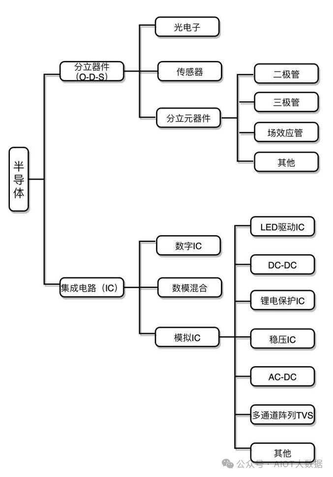
半導(dǎo)體分類
集成電路封測技術(shù)水平及特點
1. 發(fā)展概述
·自20世紀(jì)90年代以來,集成電路封裝技術(shù)快速發(fā)展,推動了電子產(chǎn)品向小型化和多功能方向邁進。
·隨著芯片結(jié)構(gòu)需求的變化,封裝技術(shù)逐步從單項技術(shù)或混合應(yīng)用技術(shù)發(fā)展為高級封裝技術(shù),以適應(yīng)下游領(lǐng)域的需求。
2. 按照封裝結(jié)構(gòu)分類的技術(shù)演進
·發(fā)展歷程:
金屬圓形封裝(TO) → 雙列直插封裝(DIP) → 塑料有引線片式載體(PLCC) → 四邊引線扁平封裝(QFP) → 針柵陣列(PGA) →球柵陣列(BGA) → 芯片尺寸封裝(CSP) →多芯片組件(MCM) → 系統(tǒng)級封裝(SIP)
·技術(shù)特點:
oDIP(雙列直插封裝):
§通用型插裝封裝,引腳從兩側(cè)引出。
§常用于傳統(tǒng)集成電路,結(jié)構(gòu)簡單,適合通孔安裝。
oPQFP(塑料方塊平面封裝):
§引腳間距小,管腳細(xì)。
§適用于大規(guī)模或超大規(guī)模集成電路(引腳數(shù)超過100)的封裝。
oTQFP(薄塑封四角扁平封裝):
§節(jié)省空間,減小體積和高度。
§適用于對散熱要求較高的集成電路產(chǎn)品。
3. 按照連接方式分類的技術(shù)演進
·引線鍵合(WB)→載帶自動鍵合(TAB)→倒裝芯片鍵合(Flip Chip)→硅通孔(TSV)。
4. 按照裝配方式分類的技術(shù)演進
·通孔插裝(THT)→表面組裝(SMT)→直接安裝(DCA)。
5. 傳統(tǒng)封裝與先進封裝
·傳統(tǒng)封裝:
o代表技術(shù):DIP、SOT、SOP等。
o優(yōu)勢:成熟工藝,成本較低。
o劣勢:體積較大,性能受限。
·先進封裝:
o技術(shù)路徑:
1.晶圓級芯片封裝(WLCSP):
§扇入型封裝(Fan-In):適合單芯片小體積應(yīng)用。
§扇出型封裝(Fan-Out):引腳密度高,性能提升。
§倒裝(Flip Chip):提高電氣性能,適合高頻應(yīng)用。
2.系統(tǒng)級封裝(SIP):
§將多個裸片封裝在一起,集成不同功能模塊。
§提高集成度,適用于復(fù)雜系統(tǒng)需求。
·先進封裝的優(yōu)勢:
o更高的性能、更低的功耗。
o滿足現(xiàn)代電子產(chǎn)品的高集成化和多功能需求。
6. 國內(nèi)封測行業(yè)現(xiàn)狀
·國內(nèi)一流封測廠商已掌握多項先進封裝技術(shù)。
·中小規(guī)模廠商在傳統(tǒng)封裝技術(shù)基礎(chǔ)上,不斷投入研發(fā)資源,探索先進封裝技術(shù)。
·未來發(fā)展方向:重點研發(fā)晶圓級封裝與系統(tǒng)級封裝。
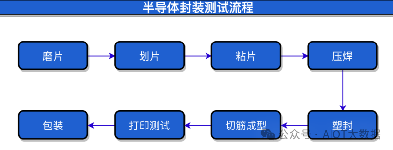
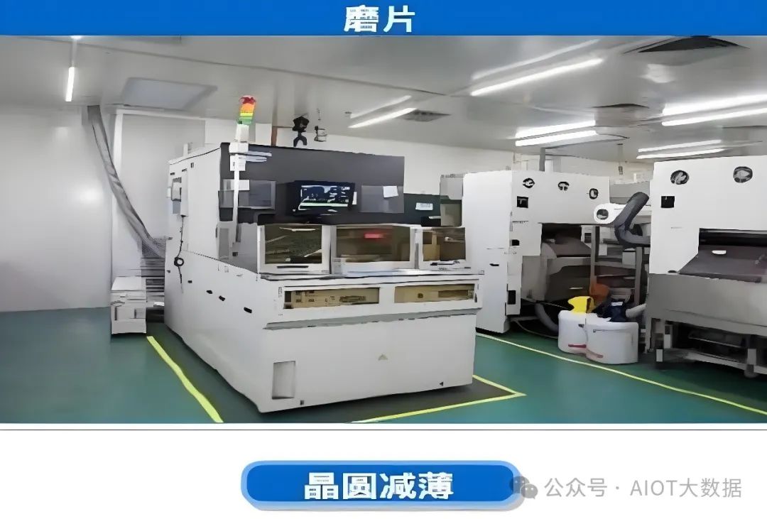
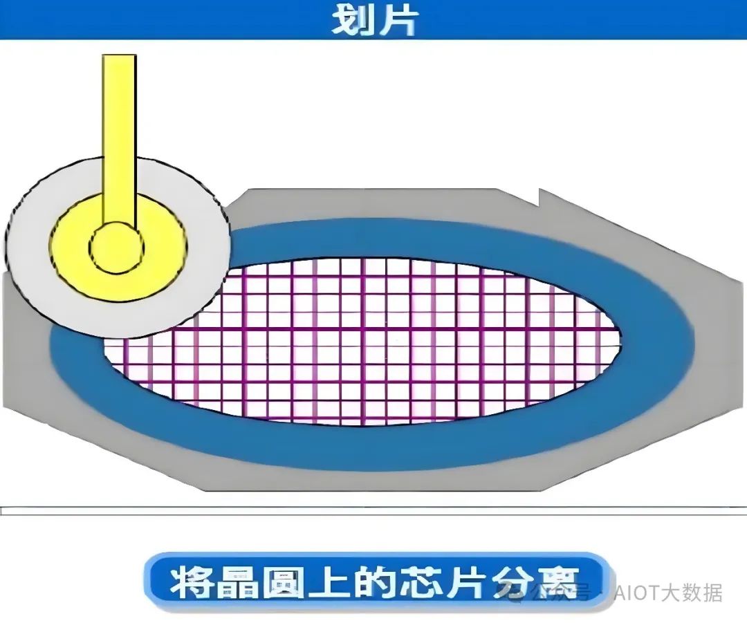
半導(dǎo)體封裝測試流程
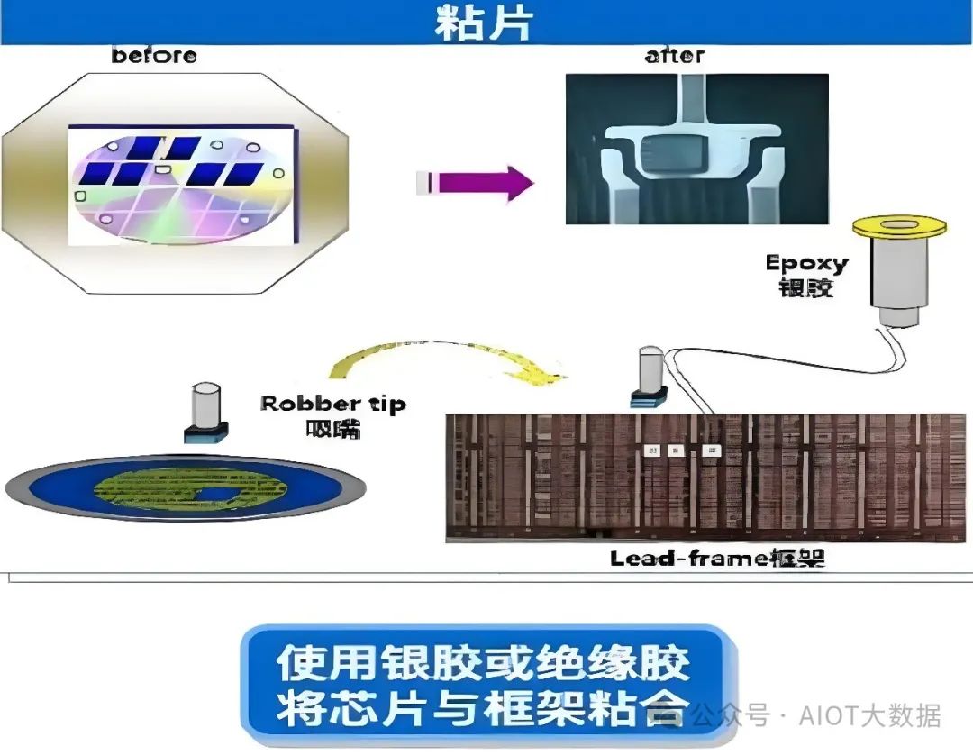
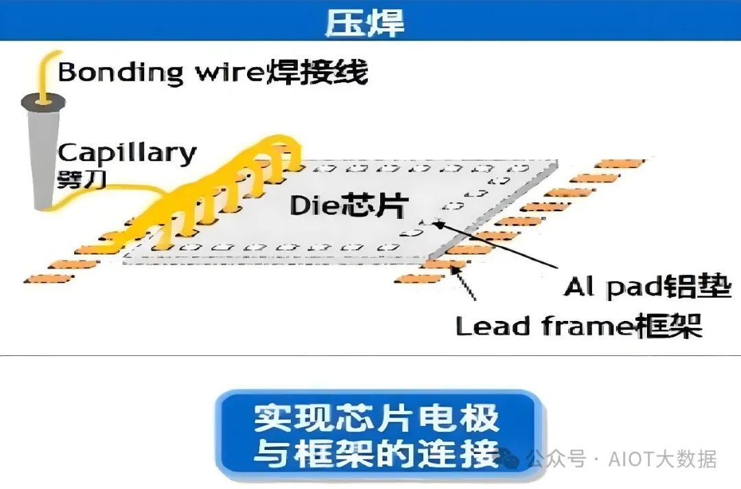
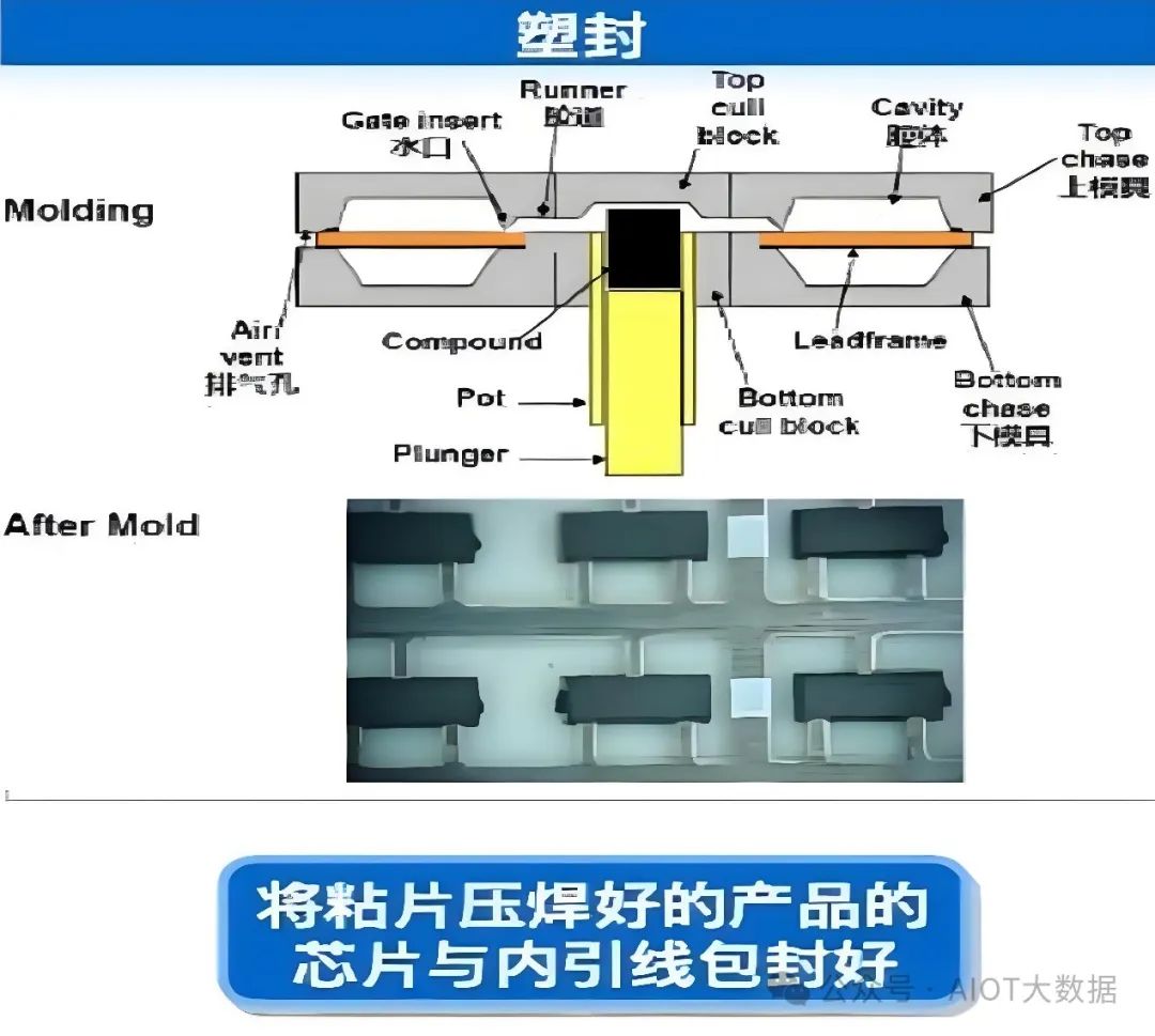
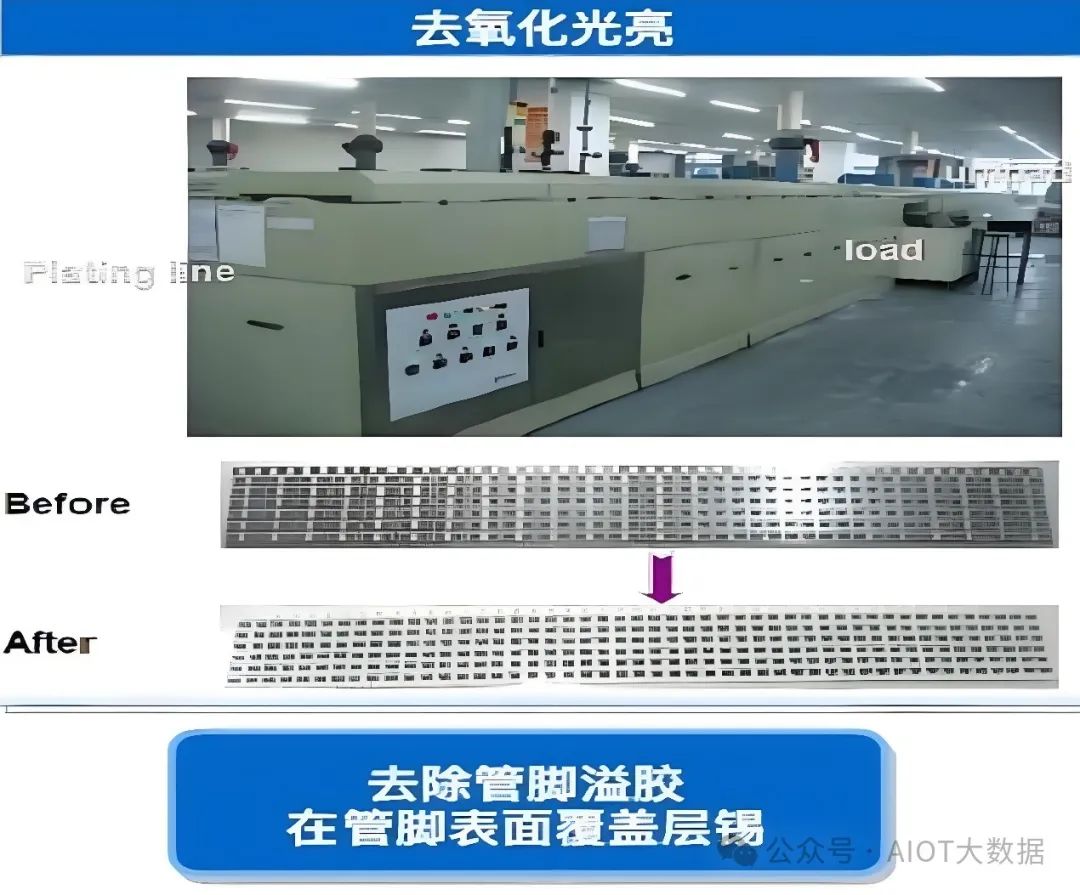
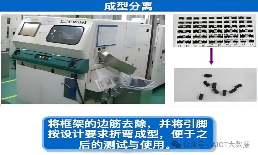
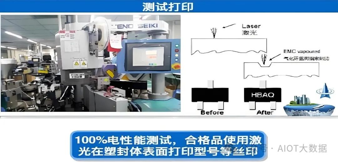
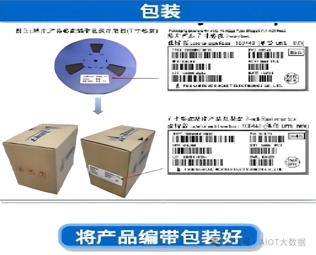
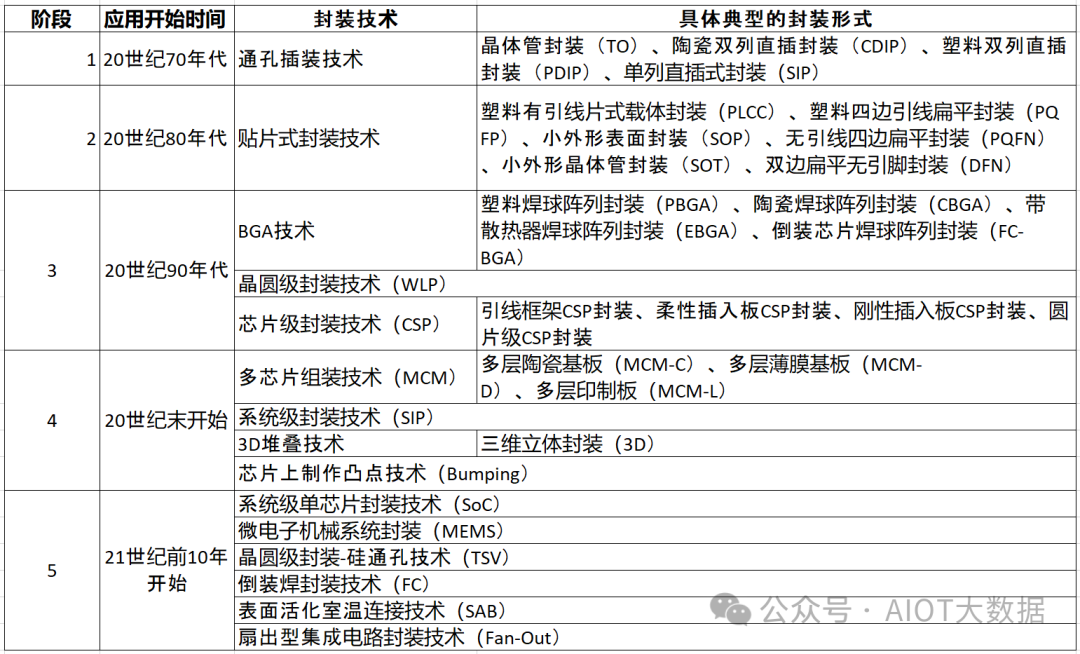
半導(dǎo)體封測發(fā)展歷史
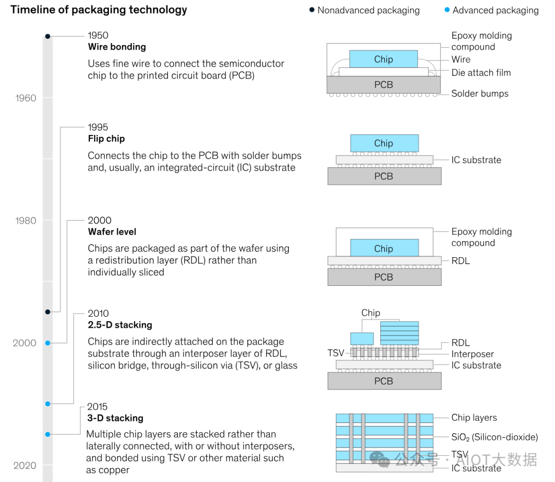
A Comprehensive Comparison of IC Packaging Interconnect Technologies
IC封裝互連技術(shù)綜合比較
INTRODUCTION介紹
When it comes toIC packageinterconnect selection, design engineers need to factor-in a host of complex issues, including cost, performance, end-use applications and much more. Two predominant technologies, Flip Chip and Wire Bonding, are popular interconnect options connecting ICs to packages or substrates.
在選擇IC 封裝互連時,設(shè)計工程師需要考慮許多復(fù)雜的問題,包括成本、性能、最終用途應(yīng)用等。倒裝芯片和引線鍵合這兩種主要技術(shù)是將 IC 連接到封裝或基板的流行互連選項。
Both bonding techniques play a crucial role in the fabrication and performance of electronic devices, while each presents its own unique advantages and challenges. This article compares in detail many critical factors influencing the selection of the optimal IC package interconnect option as it relates to a variety of different performance requirements.
這兩種鍵合技術(shù)在電子設(shè)備的制造和性能中都發(fā)揮著至關(guān)重要的作用,同時每種技術(shù)都有其獨特的優(yōu)勢和挑戰(zhàn)。本文詳細(xì)比較了影響最佳 IC 封裝互連選項選擇的許多關(guān)鍵因素,因為它涉及各種不同的性能要求。
MAIN CHARACTERISTICS:主要特點:
| Feature特征 | Wire Bonding打線鍵合 | Flip Chip倒裝芯片 |
|
GeneralDescription 一般說明 |
Wire Bonding is a long-standing and popular interconnection method, that uses thin metallic bond wires, typically made of gold, aluminum or copper, that are thermally or ultrasonically connected to chip terminals on one end, and the package pins orPCBon the other end. 引線鍵合是一種長期流行的互連方法,它使用細(xì)金屬鍵合線,通常由金、鋁或銅制成,一端通過熱或超聲波連接到芯片端子,另一端連接到封裝引腳或PCB結(jié)尾。 |
Flip Chip, AKA Controlled Collapse Chip Connection (C4), is an advanced packaging technology whereby the chip is flipped upside-down and connected directly to the substrate using small solder bumps. Bumps serve as electrical and mechanical connections between the chip and the substrate. 倒裝芯片,又稱受控塌陷芯片連接 (C4),是一種先進的封裝技術(shù),將芯片上下翻轉(zhuǎn)并使用小焊料凸塊直接連接到基板。凸塊充當(dāng)芯片和基板之間的電氣和機械連接。 |
| Bonding Types粘合類型 |
Two main types of Wire Bonding: 引線鍵合的兩種主要類型: ·Ball Bonding: Process typically uses gold wire. A small ball is formed at the end of the wire and attached to the bond pad using heat and pressure. The other end of the wire is then connected to the chip package using ultrasonic energy. ·球焊:工藝通常使用金線。在導(dǎo)線末端形成一個小球,并通過熱量和壓力將其附著到焊盤上。然后使用超聲波能量將電線的另一端連接到芯片封裝。 ·Wedge Bonding: Process often uses aluminum wire. The wire is threaded through a capillary and pressed against the bond pad without forming a ball. It can be done at room temperature. ·楔焊:工藝通常使用鋁線。導(dǎo)線穿過毛細(xì)管并壓在焊盤上,但不形成球。它可以在室溫下完成。 |
Types of Flip Chip Bumping: 倒裝芯片凸塊類型: There are numerous methods that can be used in creating the solder bumps on Flip Chips: 有多種方法可用于在倒裝芯片上創(chuàng)建焊料凸塊: ·Screen printing絲網(wǎng)印刷 ·Electroplating電鍍 ·Electroless plating化學(xué)鍍 ·Evaporation蒸發(fā) ·Solder bump with wire bonder 使用焊線機焊接凸塊 |
|
Bonding粘合 Process過程 |
Wire Bonding process key steps: 引線鍵合工藝關(guān)鍵步驟: ·Substrate preparation – cleaning and applying adhesive 基材準(zhǔn)備 – 清潔和涂抹粘合劑 ·Careful placement and alignment of the semiconductor chip 半導(dǎo)體芯片的仔細(xì)放置和對準(zhǔn) ·Positioning of the wire for bonding 接合線的定位 ·Bonding the wire to the bond pad using either ball or wedge bonding technique 使用球焊或楔焊技術(shù)將導(dǎo)線焊接至焊盤 ·Trimming the wire to the desired length 將電線修剪至所需長度 ·Optional encapsulation for protection 可選封裝保護 |
Flip Chip process key steps: 倒裝芯片工藝關(guān)鍵步驟: ·Formation of solder bumps on chip bond pads 在芯片焊盤上形成焊料凸塊 ·Flipping the chip and aligning it with the substrate 翻轉(zhuǎn)芯片并將其與基板對齊 ·Reflowing the solder to create the connections 回流焊料以形成連接 Underfilling the space between the chip and substrate for mechanical stability. Underfill materials are adhesives that are introduced between the flip-chip die and the substrate. They are configured to match the CTE of interconnect and distribute the stresses on interconnect solder joints. 對芯片和基板之間的空間進行底部填充,以實現(xiàn)機械穩(wěn)定性。底部填充材料是在倒裝芯片芯片和基板之間引入的粘合劑。它們被配置為匹配互連的 CTE 并分布互連焊點上的應(yīng)力。 |
| Advantages優(yōu)點 |
Advantages of Wire Bonding: 引線鍵合的優(yōu)點: ·Cost-effective:relatively inexpensive and mature semiconductor interconnection method 成本效益:相對便宜且成熟的半導(dǎo)體互連方法 ·Versatile:Used for a wide range of chip sizes and applications, although not leading-edge 多功能:用于各種芯片尺寸和應(yīng)用,盡管不是前沿的 ·Traditional process:Wire Bonding equipment and processes are mature and widely available 傳統(tǒng)工藝:引線鍵合設(shè)備和工藝成熟且廣泛應(yīng)用 ·Flexible:Allowing for easy changes in design and quick turnaround times. 靈活:可以輕松更改設(shè)計并縮短周轉(zhuǎn)時間。 |
Advantages of Flip Chip:倒裝芯片的優(yōu)點: ·Higher I/O density:Allows for more connections in a smaller area 更高的 I/O 密度:允許在更小的區(qū)域內(nèi)進行更多的連接 ·Good electrical performance:Shorter interconnect lengths allow lower parasitic (stray capacitance) 良好的電氣性能:較短的互連長度可降低寄生(雜散電容) ·Better thermal performance:Direct contact between the chip and substrate improves heat dissipation 更好的熱性能:芯片與基板直接接觸,提高散熱效果 ·Smaller form factor:For more compact electronic device designs 更小的外形尺寸:適合更緊湊的電子設(shè)備設(shè)計 ·Potential for 3D integration:Vertical chip stacking 3D 集成的潛力:垂直芯片堆疊 |
| Challenges挑戰(zhàn) |
Challenges of Wire Bonding: 引線鍵合的挑戰(zhàn): ·Lower I/O density compared to Flip Chip 與倒裝芯片相比,I/O 密度更低 ·Longer interconnect lengths that can hamper electrical performance 較長的互連長度可能會影響電氣性能 ·Larger chip footprint due to the need for bond pads around the periphery of the chip 由于芯片外圍需要焊盤,因此芯片占用空間更大 ·Limited in high-frequency applications due to high parasitic (stray capacitance) effects 由于高寄生(雜散電容)效應(yīng),在高頻應(yīng)用中受到限制 |
Challenges of Flip Chip:倒裝芯片的挑戰(zhàn): ·Process can be more complex and costly compared with Wire Bonding 與引線鍵合相比,工藝可能更復(fù)雜且成本更高 ·Requires precise alignment during assembly 組裝時需要精確對準(zhǔn) ·Any thermal expansion mismatch between chip and substrate can cause reliability issues 芯片和基板之間的任何熱膨脹不匹配都可能導(dǎo)致可靠性問題 ·Rework can be more involved compared with Wire Bonded packages 與引線鍵合封裝相比,返工可能更多 |
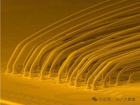
Figure 1: Wirebond wires in packages. Source: K&S
圖 1:封裝中的引線鍵合線。來源:K&S
PERFORMANCE & OPTIMIZATION COMPARISON:
性能和優(yōu)化比較:
Electrical Performance:Flip Chip technology generally offers the superior electrical performance option due to its shorter interconnection lengths. This results in lower parasitic resistance, inductance, and capacitance.
電氣性能:倒裝芯片技術(shù)由于其較短的互連長度,通常提供卓越的電氣性能選擇。這會降低寄生電阻、電感和電容。
Wire Bonding, while not as efficient, can still achieve good performance for many applications, especially when using design recommendations such as:
引線鍵合雖然效率不高,但仍然可以在許多應(yīng)用中實現(xiàn)良好的性能,特別是在使用以下設(shè)計建議時:
oIdentifying and optimizing critical signals
識別和優(yōu)化關(guān)鍵信號
oPaying careful attention to die pad ring design and placement
仔細(xì)注意芯片焊盤環(huán)的設(shè)計和放置
oSelecting the most suitable wire bond diameter
選擇最合適的焊線直徑
oOptimizing substrate signal path connectivity
優(yōu)化基板信號路徑連接
Thermal Performance:Flip Chip packages typically have better thermal performance due to the direct contact between chip and substrate. However, wire bonded packages can improve upon thermal performance by implementing the following:
熱性能:由于芯片和基板之間的直接接觸,倒裝芯片封裝通常具有更好的熱性能。然而,引線接合封裝可以通過實施以下措施來提高熱性能:
oAdding a thermal ball matrix in BGA packages
在 BGA 封裝中添加熱球矩陣
oIncreasing the substrate layer count
增加基材層數(shù)
oMaximizing the via count on the die attach pad
最大化芯片連接墊上的通孔數(shù)量
oBeefing up copper plane thickness
增加銅平面厚度
oEmploying heatsinks, slugs, etc.
使用散熱器、散熱片等。
oUtilizing filled vias利用填充過孔
Size & Density:Flip Chip technology allows for higher I/O density and smaller package sizes. Wire Bonding requires more space due to the need for bond pads around the chip periphery and the arc of the wire bonds. However, Wire Bonding can still achieve high density in some applications through techniques like staggered bond pad arrangements.
尺寸和密度:倒裝芯片技術(shù)可實現(xiàn)更高的 I/O 密度和更小的封裝尺寸。由于需要圍繞芯片外圍的焊盤和引線鍵合的弧度,引線鍵合需要更多的空間。然而,在某些應(yīng)用中,引線鍵合仍然可以通過交錯鍵合焊盤排列等技術(shù)實現(xiàn)高密度。
Cost Considerations:A cost comparison between Wire Bonding and Flip Chip technology is not straight-forward. Cost comparisons can be heavily influenced by type of application, case-specific issues, and additional factors such as:
成本考慮因素:引線鍵合和倒裝芯片技術(shù)之間的成本比較并不簡單。成本比較可能會受到應(yīng)用程序類型、具體案例問題以及其他因素的嚴(yán)重影響,例如:
oDie & wafer-level issues (e.g., bond pad pitch, configuration)
芯片和晶圓級問題(例如,焊盤間距、配置)
oDie cost & yield模具成本和產(chǎn)量
oType of Flip Chip bumping technology used
使用的倒裝芯片凸塊技術(shù)的類型
oPackage assembly flow封裝組裝流程
oProcess Total-Cost-of-Ownership (TCO)
流程總體擁有成本 (TCO)
oProduction volumes產(chǎn)量
Costing Overview:Wire Bonding seems the more cost-effective method for lower I/O counts and lower production volumes. In non-leading-edge applications, Wire Bonding is considered the more cost-effective of the twoIC packaginginterconnect solutions. However, Flip Chip technology becomes more the more economical option when I/O count increases and for higher production volumes; mainly due to its smaller die area, that allows for more dies per wafer at a reduced cost per unit.
成本概述:對于較少的 I/O 數(shù)量和較低的產(chǎn)量,引線鍵合似乎是更具成本效益的方法。在非前沿應(yīng)用中,引線鍵合被認(rèn)為是兩種IC 封裝互連解決方案中更具成本效益的。然而,當(dāng) I/O 數(shù)量增加且產(chǎn)量更高時,倒裝芯片技術(shù)就成為更經(jīng)濟的選擇;主要是由于其芯片面積較小,因此每個晶圓可以容納更多芯片,同時降低單位成本。
Manufacturability:When it comes to manufacturing process compatibility and ease of assembly, Wire Bonding remains the more flexible option, allowing for fewer complex design changes and faster turnaround times. Flip Chip requires more precise alignment and involves a more complex assembly process. However, in high-volume production, Flip Chip is more advantageous due to its potential for increased productivity.
可制造性:在制造工藝兼容性和組裝簡易性方面,引線鍵合仍然是更靈活的選擇,可以減少復(fù)雜的設(shè)計更改并縮短周轉(zhuǎn)時間。倒裝芯片需要更精確的對準(zhǔn),并涉及更復(fù)雜的組裝過程。然而,在大批量生產(chǎn)中,倒裝芯片由于其提高生產(chǎn)率的潛力而更具優(yōu)勢。
Reliability:When properly implemented, both technologies can achieve high reliability. Wire Bonding boasts an established history of proven reliability for a wide range of applications. Flip Chip however provides outstanding reliability, particularly in harsh environments, due to shorter interconnects and underfill. Underfills areused for mechanical stabilization and protection, compensating for material stresses and reducing coefficient of thermal expansion (CTE), in electronic assemblies, especially Flip Chips.
可靠性:如果實施得當(dāng),這兩種技術(shù)都可以實現(xiàn)高可靠性。引線鍵合擁有在各種應(yīng)用中經(jīng)過驗證的可靠性的悠久歷史。然而,由于更短的互連和底部填充,倒裝芯片提供了出色的可靠性,特別是在惡劣的環(huán)境中。底部填充膠用于電子組件(尤其是倒裝芯片)中的機械穩(wěn)定性和保護、補償材料應(yīng)力并降低熱膨脹系數(shù) (CTE)。
At a Glance Comparison:概覽比較:
| Feature特征 | Flip Chip倒裝芯片 | Wire Bond焊線 |
| I/O Density輸入/輸出密度 |
HigherI/O density, allows smaller, more compact chip packages, resulting in increased functionality. 更高的 I/O 密度可實現(xiàn)更小、更緊湊的芯片封裝,從而增強功能。 |
LowerI/O density, requires larger chip package sizes, with lower functionality. I/O 密度較低,需要較大的芯片封裝尺寸,且功能較低。 |
|
Interconnect互連 Length長度 |
Shorter interconnectlengths allow better electrical performance andlower ‘parasitic’ or (stray capacitance). 較短的互連長度可實現(xiàn)更好的電氣性能和更低的“寄生”或(雜散電容)。 |
Longer, thinnerinterconnectlengths due to wires, result in less effective electrical performance and higher ‘parasitic’ or (stray capacitance). 由于電線而導(dǎo)致互連長度更長、更細(xì),導(dǎo)致有效的電氣性能降低和更高的“寄生”或(雜散電容)。 |
| Heat Dissipation散熱 |
Improved heat dissipation, reduces the risk of overheating. 改善散熱,降低過熱風(fēng)險。 |
Less effective heat dissipationdue to limited surface area for heat transfer. 由于傳熱表面積有限,散熱效果較差。 |
| Package Size包裝尺寸 |
Smaller chip packages,allows for smaller electronic devices. Vertical stacking and 3D IC integration are easily achieved. 更小的芯片封裝允許更小的電子設(shè)備。可以輕松實現(xiàn)垂直堆疊和 3D IC 集成。 |
Wires between chip and bond pad can be longer, resulting in alarger footprint. Vertical stacking is far more complex. 芯片和焊盤之間的電線可以更長,從而導(dǎo)致更大的占地面積。垂直堆疊要復(fù)雜得多。 |
| Design設(shè)計 |
More design complexity due to higher interconnection density. Requires precise alignment of pitch pads and solder bumps. 由于互連密度更高,設(shè)計變得更加復(fù)雜。需要精確對準(zhǔn)間距焊盤和焊料凸塊。 |
Simpler designdue to fewer I/O connections and less precision needed to attach wires to the bond pads. 由于 I/O 連接較少,并且將導(dǎo)線連接到焊盤所需的精度較低,因此設(shè)計更加簡單。 |
| Costing成本核算 |
At high volume and high manufacturing yieldsflip-chip can be more cost effective. The smaller die area fits more dies per wafer, reducing cost per unit. 在大批量和高制造產(chǎn)量的情況下,倒裝芯片可以更具成本效益。較小的芯片面積可以在每個晶圓上容納更多的芯片,從而降低單位成本。 |
For non-leading-edge applications Wire Bonding is themost likely cost-effective packaging solution. 對于非前沿應(yīng)用,引線鍵合是最有可能具有成本效益的封裝解決方案。 |
| Process Nodes流程節(jié)點 |
Can be used foradvanced process nodesin the rage of 7nm / 5nm. 可用于7nm/5nm時代的先進工藝節(jié)點。 |
Can be used formoremature process nodes, in the rage 28nm / 14nm. 可用于更成熟的工藝節(jié)點,流行的有28nm/14nm。 |
USE-CASES & APPLICATIONS用例和應(yīng)用
Common Wire Bonding Applications:This basic technique is widely used in microelectronic products for a wide range of industries and applications, mainly because of its cost-efficiency, versatility and reliability:
常見引線鍵合應(yīng)用:這種基本技術(shù)廣泛應(yīng)用于各種行業(yè)和應(yīng)用的微電子產(chǎn)品,主要是因為其成本效益、多功能性和可靠性:
oIntegrated Circuits (ICs): Wire Bonding is still the dominant technology used in connecting IC chips to packages, especially for mature process nodes (28nm and above).
集成電路 (IC):引線鍵合仍然是連接IC 芯片與封裝的主要技術(shù),特別是對于成熟的工藝節(jié)點(28 納米及以上)。
oSensors: Many sensory devices, such as pressure sensors, temperature sensors, and accelerometers, use Wire Bonding for electrical connections.
傳感器:許多傳感設(shè)備,例如壓力傳感器、溫度傳感器和加速度計,都使用引線鍵合進行電氣連接。
oOptoelectronics: Devices like LEDs, photodiodes, and laser diodes regularly use Wire Bonding for electrical and optical signal transmission connections.
光電器件:LED、光電二極管和激光二極管等器件經(jīng)常使用引線鍵合進行電信號和光信號傳輸連接。
oPower Devices: MOSFETs and insulated gate bipolar transistors (IGBTs) frequently use Wire Bonding for power connections.
功率器件:MOSFET 和絕緣柵雙極晶體管 (IGBT) 經(jīng)常使用引線鍵合進行電源連接。
oMemory Devices: Many memory chips, especially those not requiring super high performance, use Wire Bonding.
存儲器件:許多存儲芯片,尤其是那些不需要超高性能的存儲芯片,都使用引線鍵合。
Common Flip Chip Applications:In answer to market demand for quality high-speed and high-performance package design, the most commonly used packaging solution for these more advanced applications is flip chip technology:
常見的倒裝芯片應(yīng)用:為了滿足市場對高質(zhì)量高速和高性能封裝設(shè)計的需求,這些更先進的應(yīng)用最常用的封裝解決方案是倒裝芯片技術(shù):
oHigh-Performance Processors: CPUs and GPUs for computers and servers require Flip Chip technology to achieve the highest performance and I/O density.
高性能處理器:計算機和服務(wù)器的 CPU 和 GPU 需要倒裝芯片技術(shù)來實現(xiàn)最高的性能和 I/O 密度。
oAdvanced Mobile Devices: Smartphones and tablets increasingly use Flip Chip technology in their main processors and other high-performance components.
先進移動設(shè)備:智能手機和平板電腦越來越多地在其主處理器和其他高性能組件中使用倒裝芯片技術(shù)。
oNetworking Equipment: High-speed routers and switches need the kind of improved electrical performance Flip Chip packaging can deliver.
網(wǎng)絡(luò)設(shè)備:高速路由器和交換機需要倒裝芯片封裝能夠提供的改進電氣性能。
oAutomotive Electronics: Advanced driver assistance systems (ADAS) and other high-performance automotive electronics are readily adopting Flip Chip technology. See also:Automotive PCBs
汽車電子:先進駕駛輔助系統(tǒng)(ADAS)和其他高性能汽車電子很容易采用倒裝芯片技術(shù)。另請參閱:汽車 PCB
oHigh-Frequency RF Devices: The shorter interconnects in Flip Chip technology make it an ideal solution for high-frequency applications in wireless communications.
高頻射頻器件:倒裝芯片技術(shù)中較短的互連使其成為無線通信中高頻應(yīng)用的理想解決方案。
EYE ON THE FUTURE著眼未來
Monitoring Future Trends:Both Wire Bonding and Flip Chip continue to evolve, with a view towards meet pressing market demand for vastly improved near-future electronic device technology.
監(jiān)控未來趨勢:引線鍵合和倒裝芯片都在不斷發(fā)展,以滿足市場對近期電子設(shè)備技術(shù)大幅改進的迫切需求。
| Wire Bonding Trends引線鍵合趨勢 | Flip Chip Trends倒裝芯片趨勢 |
|
Development of finer pitch bonding capabilities 開發(fā)更細(xì)間距的接合能力 Alternative wire materials (e.g., copper) for improved performance and costing 替代電線材料(例如銅)可提高性能和成本 Advancements in equipment and process control for higher efficiency and reliability 設(shè)備和過程控制的進步提高了效率和可靠性 |
Continued miniaturization of solder bumps for even higher I/O densities 焊料凸點持續(xù)小型化,以實現(xiàn)更高的 I/O 密度 Development of advanced underfill materials for improved reliability 開發(fā)先進的底部填充材料以提高可靠性 Integration with other advanced packaging technologies, such as 2.5D and 3D 與其他先進封裝技術(shù)集成,例如 2.5D 和 3D |
Final Thoughts:The choice between Wire Bonding and Flip Chip depends on various factors, including electrical and thermal requirements, size constraints, production volume, and cost considerations. As the electronics industry continues to demand higher performance and smaller form factors, both technologies will likely coexist, with each finding its niche in different applications and market segments.
最后的想法:引線鍵合和倒裝芯片之間的選擇取決于多種因素,包括電氣和熱要求、尺寸限制、產(chǎn)量和成本考慮。隨著電子行業(yè)不斷要求更高的性能和更小的外形尺寸,這兩種技術(shù)可能會共存,每種技術(shù)都會在不同的應(yīng)用和細(xì)分市場中找到自己的定位。
As the benefits of Moore’s law reach their limits, advances in chip performance rely more on the back end of production, including packaging.
隨著摩爾定律的優(yōu)勢達到極限,芯片性能的進步更多地依賴于包括封裝在內(nèi)的生產(chǎn)后端
Semiconductor wafers are the basisof the integrated circuits so crucial to most of today’s technology. The wafers’ packaging—whether metal, plastic, ceramic, or glass—connects them to their environment and protects them from chemical contamination and damage from light, heat, and impacts. Compared with the front-end process of designing and fabricating wafers, the back-end process of packaging has been undervalued for two reasons: First, it’s still possible to package wafers using old-generation equipment. Second, packaging is mostly done by outsourced semiconductor assembly and test companies (OSATs) that compete largely based on low labor costs, rather than other sources of differentiation.
半導(dǎo)體晶圓是集成電路的基礎(chǔ),對當(dāng)今大多數(shù)技術(shù)至關(guān)重要。晶圓的包裝(無論是金屬、塑料、陶瓷還是玻璃)將它們與環(huán)境連接起來,并保護它們免受化學(xué)污染以及光、熱和沖擊造成的損壞。與設(shè)計和制造晶圓的前端工藝相比,封裝的后端工藝被低估,原因有二:首先,仍然可以使用老一代設(shè)備來封裝晶圓。其次,封裝主要由外包半導(dǎo)體組裝和測試公司(OSAT)完成,這些公司主要基于低勞動力成本而不是其他差異化來源進行競爭。
This model may change with the introduction of advanced packaging, which uses sophisticated technology and aggregates components from various wafers, creating a single electronic device with superior performance. Introduced around 2000, advanced packaging is now gaining significant momentum as the next breakthrough in semiconductor technology.
這種模式可能會隨著先進封裝的引入而改變,先進封裝使用復(fù)雜的技術(shù)并聚合來自各種晶圓的組件,創(chuàng)造出具有卓越性能的單一電子設(shè)備。先進封裝于 2000 年左右推出,目前作為半導(dǎo)體技術(shù)的下一個突破正在獲得巨大的發(fā)展勢頭。
Advanced packaging is helping to meet the demand for semiconductors that run emerging applications now going mainstream—for example, 5G, autonomous vehicles and other Internet of Things technologies, and virtual and augmented reality. These applications require high-performance, low-power chips that can rapidly process massive quantities of data. Despite Moore’s law, which in 1965 posited that the number of transistors on a microchip would double every couple of years, node advancement is now reaching its limits. As a result, technical advances on the front end of chip manufacturing are slowing, and the economically viable maximum size of a die, and thus its performance, are becoming more limited. New approaches in back-end technology that combine multiple chips offer a promising solution. Advanced-packaging techniques that have arisen over the past two decades—including 2.5-D, 3-D, fan-out, and system-on-a-chip (SoC) packaging—promise to fill the void by supplementing the wire-bonding and flip-chip technologies of the previous half century.
先進封裝有助于滿足對運行現(xiàn)已成為主流的新興應(yīng)用(例如 5G、自動駕駛汽車和其他物聯(lián)網(wǎng)技術(shù)以及虛擬和增強現(xiàn)實)的半導(dǎo)體的需求。這些應(yīng)用需要高性能、低功耗的芯片,能夠快速處理大量數(shù)據(jù)。盡管摩爾定律在 1965 年規(guī)定微芯片上的晶體管數(shù)量每隔幾年就會翻一番,但節(jié)點的進步現(xiàn)在已經(jīng)達到了極限。因此,芯片制造前端的技術(shù)進步正在放緩,經(jīng)濟上可行的芯片最大尺寸及其性能也變得更加有限。結(jié)合多個芯片的后端技術(shù)新方法提供了一個有前途的解決方案。過去二十年出現(xiàn)的先進封裝技術(shù)(包括 2.5D、3D、扇出和片上系統(tǒng) (SoC) 封裝)有望通過補充引線鍵合來填補空白以及前半個世紀(jì)的倒裝芯片技術(shù)。
Because advanced packaging offers a higher-value opportunity than traditional back-end packaging, major players and fast followers (organizations that imitate competitors’ innovations) are developing and commercializing various forms of the technology to win premium customers. In this article, we describe how the market is evolving and suggest how manufacturers can take advantage of the opportunities becoming available.
由于先進封裝提供了比傳統(tǒng)后端封裝更高價值的機會,因此主要參與者和快速追隨者(模仿競爭對手創(chuàng)新的組織)正在開發(fā)各種形式的技術(shù)并將其商業(yè)化,以贏得優(yōu)質(zhì)客戶。
Key advanced-packaging technologies
先進封裝關(guān)鍵技術(shù)
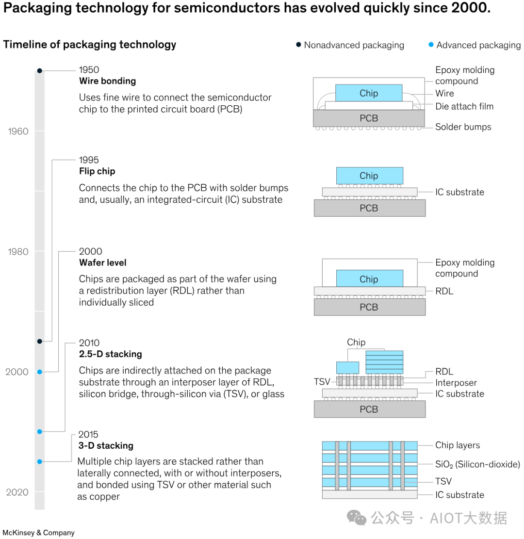
Three major advanced-packaging technologies have become commercially available since 2000, supplementing the two technologies that prevailed during the previous half century (Exhibit 1).
自 2000 年以來,三種主要的先進封裝技術(shù)已投入商業(yè)應(yīng)用,補充了過去半個世紀(jì)盛行的兩種技術(shù)(圖表 1)。
Traditional packaging techniques
傳統(tǒng)包裝技術(shù)
Developed in the 1950s and still in use today, wire-bond technology is an interconnection technique that attaches the printed circuit board (PCB) to the die—the silicon square that contains the integrated circuit—using solder balls and thin metal wires. It requires less space than packaged chips and can connect relatively distant points, but it can fail in high temperatures, high humidity, and temperature cycling, and each bond must be formed sequentially, which adds complexity and can slow manufacturing. The wire-bonding market is expected to be valued at about $16 billion by 2031, with a CAGR of 2.9 percent.
引線鍵合技術(shù)開發(fā)于 20 世紀(jì) 50 年代,至今仍在使用,它是一種互連技術(shù),使用焊球和細(xì)金屬線將印刷電路板 (PCB) 連接到芯片(包含集成電路的硅方塊)。它比封裝芯片需要更少的空間,并且可以連接相對較遠(yuǎn)的點,但它可能會在高溫、高濕度和溫度循環(huán)中失效,并且每個鍵必須順序形成,這增加了復(fù)雜性并會減慢制造速度。預(yù)計到 2031 年,引線鍵合市場價值將達到約 160 億美元,復(fù)合年增長率為 2.9%。
The first major evolution in packaging technology came in the mid-1990s with flip chips, which use a face-down die, the entire surface area of which is used for interconnection through solder “bumps” that bond the PCB with the die. This results in a smaller form factor, or hardware size, and a higher signal-propagation rate—that is, faster movement of signals from the transmitter to the receiver. Flip-chip packaging is the most common and lowest-cost technology currently in use, mainly for central processing units, smartphones, and radio-frequency system-in-package solutions. Flip chips allow for smaller assembly and can handle higher temperatures, but they must be mounted on very flat surfaces and are not easy to replace. The current flip-chip market is around $27 billion, with a projected CAGR of 6.3 percent, which should bring it to $45 billion by 2030.
封裝技術(shù)的第一次重大發(fā)展出現(xiàn)在 20 世紀(jì) 90 年代中期的倒裝芯片中,它使用面朝下的芯片,其整個表面區(qū)域用于通過將 PCB 與芯片粘合的焊料“凸塊”進行互連。這導(dǎo)致更小的外形尺寸或硬件尺寸以及更高的信號傳播速率,即信號從發(fā)射器到接收器的更快移動。倒裝芯片封裝是目前使用最常見、成本最低的技術(shù),主要用于中央處理器、智能手機和射頻系統(tǒng)級封裝解決方案。倒裝芯片允許更小的組裝并且可以承受更高的溫度,但它們必須安裝在非常平坦的表面上并且不容易更換。當(dāng)前倒裝芯片市場規(guī)模約為 270 億美元,預(yù)計復(fù)合年增長率為 6.3%,到 2030 年將達到 450 億美元.
Wafer-level packaging晶圓級封裝
While traditional packaging “dices” the silicon wafer into individual chips first and then attaches the chips to the PCB and builds the electrical connections, wafer-level packaging makes the electrical connections and molding at the wafer level, then dices the chips using a laser. The greatest difference between wafer-level chip-scale packaging (WLCSP) and flip chips in terms of chip configuration is that WLCSPs have no substrate between the die and the PCB. Instead, redistribution layers (RDLs) replace the substrate, leading to a smaller package and enhanced thermal conduction.
傳統(tǒng)封裝首先將硅晶圓“切割”成單獨的芯片,然后將芯片附著到 PCB 上并建立電氣連接,而晶圓級封裝則在晶圓級進行電氣連接和成型,然后使用激光切割芯片。晶圓級芯片級封裝 (WLCSP) 和倒裝芯片在芯片配置方面的最大區(qū)別在于,WLCSP 的芯片和 PCB 之間沒有基板。相反,重新分布層 (RDL) 取代了基板,從而縮小了封裝并增強了導(dǎo)熱性。
Wafer-level packaging is divided into two types: fan-in and fan-out. In fan-in wafer-level packaging, used mainly for low-end mobile phones that require rudimentary technology, the RDLs are routed toward the center of the die. In the fan-out version, which was introduced in 2007, the RDL and solder balls exceed the size of the die, so the chip can have more inputs and outputs while maintaining a thin profile.3Fan-out packaging comes in three types: core, high density, and ultrahigh density. Core, which is used mostly for automotive and network applications that don’t require high-end technology—such as radio frequency and infotainment chips—accounts for less than 20 percent of the almost $1.5 billion fan-out packaging market. High and ultrahigh density are mostly used for mobile applications and are expected to expand to some network and high-performance computing applications. The world’s largest maker of WLCSPs is the Taiwan Semiconductor Manufacturing Company (TSMC).
晶圓級封裝分為扇入型和扇出型兩種。在主要用于需要基本技術(shù)的低端手機的扇入式晶圓級封裝中,RDL 被布線到芯片的中心。在 2007 年推出的扇出版本中,RDL 和焊球超出了芯片的尺寸,因此芯片可以擁有更多的輸入和輸出,同時保持薄型。3扇出封裝分為三種類型:核心封裝、高密度封裝和超高密度封裝。核心主要用于不需要高端技術(shù)(例如射頻和信息娛樂芯片)的汽車和網(wǎng)絡(luò)應(yīng)用,在近 15 億美元的扇出封裝市場中所占比例不到 20%。高密度和超高密度主要用于移動應(yīng)用,預(yù)計將擴展到一些網(wǎng)絡(luò)和高性能計算應(yīng)用。全球最大的 WLCSP 制造商是臺灣積體電路制造公司 (TSMC)。
The past decade saw the development of stacked WLCSP, which allows for multiple integrated circuits in the same package and is used for both heterogeneous bonding, which integrates logic and memory chips, and memory-chip stacking. In 2.5-D stacking, two or more chips are laid side by side with an interposer connecting one die to another. There are several categories of 2.5-D stacking, based on the kind of interposer it uses:
過去十年見證了堆疊式 WLCSP 的發(fā)展,它允許在同一封裝中集成多個集成電路,并可用于集成邏輯和存儲芯片的異構(gòu)鍵合以及存儲芯片堆疊。在 2.5 維堆疊中,兩個或多個芯片并排放置,并通過中介層將一個芯片連接到另一個芯片。根據(jù)所使用的中介層類型,2.5 維堆疊可分為多種類別:
·Silicon interposers are the only type that requires TSV, or through-silicon via—a vertical electrical connection that passes through the silicon die or wafer. Silicon interposers use a stable technology that has been on the market for more than ten years, but the cost of silicon is high and requires front-end technology and manufacturing capability. TSMC’s CoWoS-S (chip on wafer on substrate) dominates the market.
硅中介層是唯一需要 TSV 或硅通孔(一種穿過硅芯片或晶圓的垂直電氣連接)的類型。硅中介層采用的是已經(jīng)上市十多年的穩(wěn)定技術(shù),但硅的成本較高,并且需要前端技術(shù)和制造能力。臺積電的CoWoS-S(基板上晶圓芯片)占據(jù)市場主導(dǎo)地位。
·Silicon bridges are relatively new. Because they use smaller amounts of silicon than traditional silicon interposers, they are thinner, which reduces power consumption and increases design flexibility. Their advantage over traditional silicon interposers is that they can enable more advanced system-level integration, so they are used for high-performance computing (HPC) such as AI. Representative technologies include Intel’s EMIB (embedded multi-die interconnect bridge) and TSMC’s CoWoS-L.
硅橋相對較新。由于它們比傳統(tǒng)硅中介層使用更少的硅,因此更薄,從而降低了功耗并提高了設(shè)計靈活性。與傳統(tǒng)硅中介層相比,它們的優(yōu)勢在于可以實現(xiàn)更先進的系統(tǒng)級集成,因此它們用于人工智能等高性能計算(HPC)。代表性技術(shù)包括英特爾的EMIB(嵌入式多芯片互連橋)和臺積電的CoWoS-L。
·Redistribution layers can also function as interposers. The greatest strength of this technology is that the photolithography process that creates RDLs allows for fine patterning, which improves speed gain and heat dissipation. TSMC’s CoWoS-R (chip-on-wafer-on-substrate RDL) is set to begin mass-volume production.
重新分布層也可以充當(dāng)中介層。該技術(shù)的最大優(yōu)勢在于,創(chuàng)建 RDL 的光刻工藝可實現(xiàn)精細(xì)圖案化,從而提高速度增益和散熱。臺積電的 CoWoS-R(晶圓上芯片 RDL)即將開始量產(chǎn)。
·Glass is also rising as a next-generation material for interposers. It offers low cost and low power loss in high-frequency bandwidths, but it may not be marketable for some time.
玻璃也正在成為下一代中介層材料。它在高頻帶寬中提供低成本和低功耗,但可能在一段時間內(nèi)無法上市。
In 3-D stacking, multiple chips are placed face down on top of one another, with or without an interposer. There are two main types of 3-D stacking. The most common type is TSV with micro-bumps (μ-bumps). The newer alternative, bumpless hybrid bonding, forms interconnections using a dielectric bond and embedded metal; it is just being explored by memory players.
在 3D 堆疊中,多個芯片面朝下堆疊在一起,無論有或沒有中介層。3D 堆疊有兩種主要類型。最常見的類型是帶有微凸塊(μ 凸塊)的 TSV。較新的替代方案是無凸點混合鍵合,使用電介質(zhì)鍵合和嵌入式金屬形成互連;它只是被記憶玩家探索而已。
How will the market evolve?
市場將如何發(fā)展?
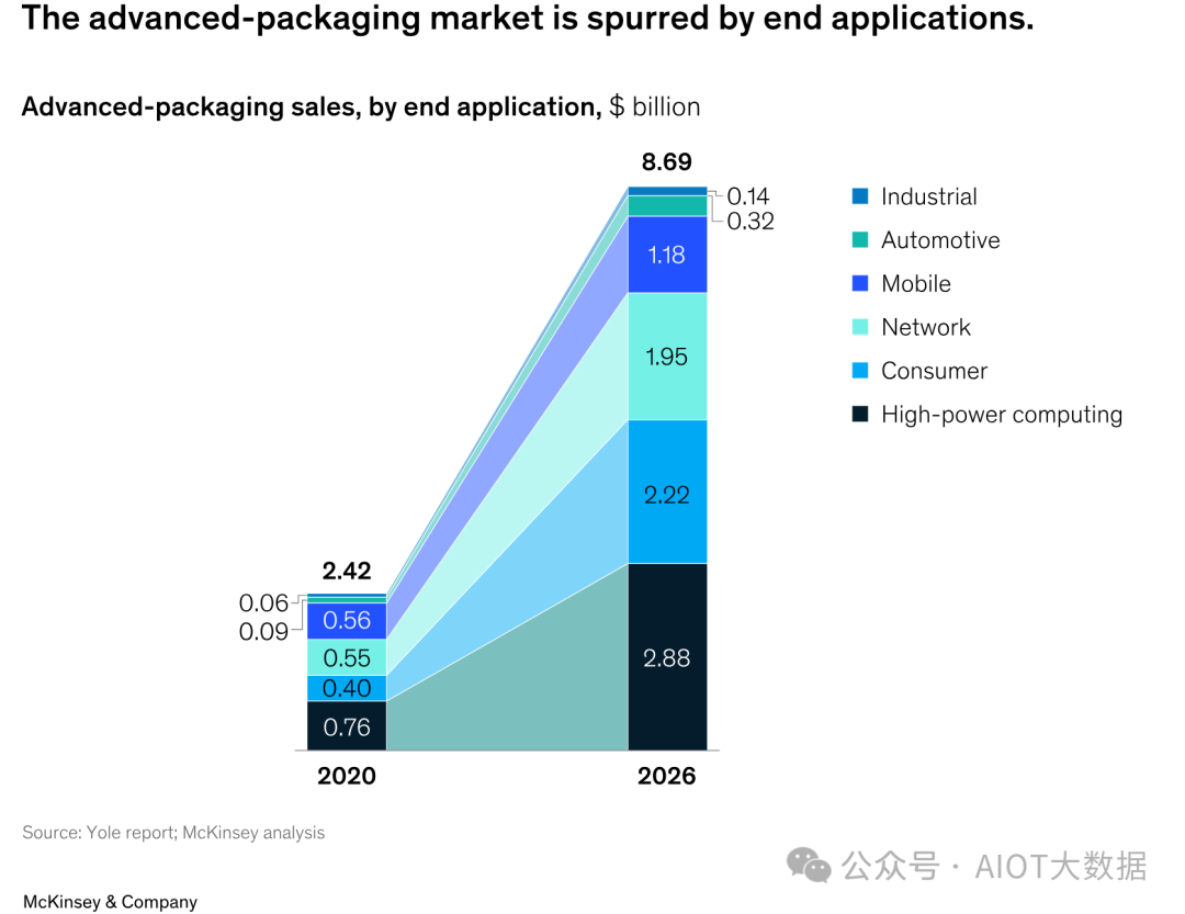
The advanced-packaging market is driven by the end applications of its various technologies (Exhibit 2). Since the mid-2010s, fan-out wafer-level packaging has dominated, with about 60 percent market share. Fan-out packaging is cheaper than stacking and is engineered for high heat resistance and a small form factor. These attributes make it appropriate for mobile applications, which are likely to generate most of its demand.
先進封裝市場由各種技術(shù)的最終應(yīng)用驅(qū)動(圖表 2)。自 2010 年代中期以來,扇出晶圓級封裝占據(jù)主導(dǎo)地位,占據(jù)約 60% 的市場份額。扇出封裝比堆疊封裝更便宜,并且專為高耐熱性和小外形而設(shè)計。這些屬性使其適合移動應(yīng)用程序,而移動應(yīng)用程序可能會產(chǎn)生大部分需求。
Apple uses fan-out advanced packaging for its application processors, graphic chips, and 5G and 6G modem chips. It is the largest user of the technology, consuming most of the volume produced by TSMC. Other top fabless players—that is, companies that design and sell hardware and chips but outsource their manufacture—are also using fan-out technology in mass-produced chips.
蘋果公司的應(yīng)用處理器、圖形芯片以及 5G 和 6G 調(diào)制解調(diào)器芯片采用扇出先進封裝。它是該技術(shù)的最大用戶,消耗了臺積電生產(chǎn)的大部分產(chǎn)量。其他頂級無晶圓廠廠商——即設(shè)計和銷售硬件和芯片但外包制造的公司——也在批量生產(chǎn)的芯片中使用扇出技術(shù)。
Most of the growth in HPC and network applications is likely to come from AI chips, edge computing, and network chips in consumer devices, which require the small form factor and affordable cost that fan-out packaging can offer.
HPC 和網(wǎng)絡(luò)應(yīng)用的大部分增長可能來自消費設(shè)備中的人工智能芯片、邊緣計算和網(wǎng)絡(luò)芯片,這些芯片需要扇出封裝能夠提供的小外形尺寸和可承受的成本。
The most likely driver of growth in 2.5-D stacking could be HPC applications, which are in high demand for data centers. Although less than 20 percent of data-center capacity used 2.5-D stacking in 2022, the rate could increase to 50 percent in the next five years. For mobile applications, 2.5-D packaging is considered too costly, but this may change with the arrival of the next generation, which will feature less expensive silicon bridges, RDLs, and glass interposers.
2.5 維堆疊增長最有可能的推動力可能是 HPC 應(yīng)用程序,數(shù)據(jù)中心對 HPC 應(yīng)用程序的需求很高。盡管到 2022 年,只有不到 20% 的數(shù)據(jù)中心容量使用 2.5 維堆疊,但這一比例在未來五年內(nèi)可能會增加到 50%。對于移動應(yīng)用,2.5D 封裝被認(rèn)為成本太高,但隨著下一代的到來,這種情況可能會改變,下一代封裝將采用更便宜的硅橋、RDL 和玻璃中介層。
For 3-D packaging, memory—the dominant application for 3-D stacking—and SoC use are expected to grow at a CAGR of roughly 30 percent. Increasingly, 3-D stacked memory is being incorporated with logic chips for high-performance products that require high bandwidth, including high-bandwidth memory (HBM) and processing in memory with HBM (PIM-HBM). Substantial demand for 3-D stacked memory will likely come from data-center servers, which require high capacity and high speed, and graphics accelerators and network devices, which require the maximum possible bandwidth for memory and processing.
對于 3D 封裝、內(nèi)存(3D 堆疊的主要應(yīng)用)和 SoC 的使用預(yù)計將以大約 30% 的復(fù)合年增長率增長。3D 堆疊存儲器越來越多地與需要高帶寬的高性能產(chǎn)品的邏輯芯片相結(jié)合,包括高帶寬存儲器 (HBM) 和采用 HBM 的存儲器處理 (PIM-HBM)。對 3D 堆棧內(nèi)存的大量需求可能來自需要高容量和高速度的數(shù)據(jù)中心服務(wù)器,以及需要盡可能大的內(nèi)存和處理帶寬的圖形加速器和網(wǎng)絡(luò)設(shè)備。
HPC systems, specifically CPUs, will drive demand for 3-D SoC chips. Major players started adopting hybrid bonding in 2022, and fast followers may join the market soon. OSATs, lower-tier foundries, and integrated device manufacturers (IDMs) are unlikely to enter the market, given the high technology barrier.
HPC 系統(tǒng),特別是 CPU,將推動對 3D SoC 芯片的需求。主要參與者于 2022 年開始采用混合粘合,快速追隨者可能很快就會加入市場。鑒于技術(shù)壁壘較高,OSAT、低端代工廠和集成設(shè)備制造商 (IDM) 不太可能進入該市場。
Key market-winning capabilities
贏得市場的關(guān)鍵能力
Market growth relies heavily on end customers, such as automotive OEMs and home appliance manufacturers. More end customers are seeking advanced-packaging providers because of the growing need for fast, reliable computing for applications such as autonomous vehicles. For semiconductor manufacturers—especially logic IDMs and foundries—advanced packaging could be a key selling point.
市場增長很大程度上依賴于最終客戶,例如汽車原始設(shè)備制造商和家電制造商。由于自動駕駛汽車等應(yīng)用對快速、可靠計算的需求不斷增長,越來越多的最終客戶正在尋求先進的封裝提供商。對于半導(dǎo)體制造商(尤其是邏輯 IDM 和代工廠)而言,先進封裝可能是一個關(guān)鍵賣點。
More end customers are seeking advanced-packaging providers because of the growing need for fast, reliable computing for applications such as autonomous vehicles.
由于自動駕駛汽車等應(yīng)用對快速、可靠計算的需求不斷增長,越來越多的最終客戶正在尋求先進的封裝提供商。
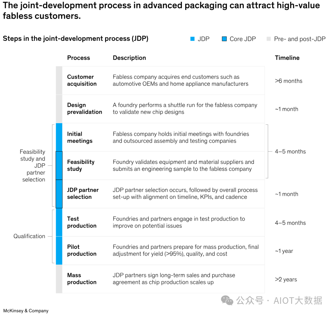
To acquire and retain high-value fabless customers, manufacturers need to be comfortable codeveloping advanced-packaging solutions. While fabless players take full ownership of the chip-planning process before at-scale production begins, there is room for manufacturers to add value. Joint development often occurs during the chip-architecture design stage and initial shuttle runs for design validation (Exhibit 3). The need for such cooperation is expected to increase because of the demand for higher-performance chips and the increased complexity of chip designs created by packaging.
為了獲得并留住高價值的無晶圓廠客戶,制造商需要輕松地共同開發(fā)先進封裝解決方案。盡管無晶圓廠廠商在大規(guī)模生產(chǎn)開始之前完全掌控了芯片規(guī)劃流程,但制造商仍有增加價值的空間。聯(lián)合開發(fā)通常發(fā)生在芯片架構(gòu)設(shè)計階段和用于設(shè)計驗證的初始穿梭運行期間(圖表 3)。由于對更高性能芯片的需求以及封裝帶來的芯片設(shè)計復(fù)雜性的增加,預(yù)計這種合作的需求將會增加。
In 2016, TSMC released innovative integrated fan-out (InFO) wafer-level systems, mainly for wireless applications, in close collaboration with its lead customer. More recently, derivatives of that, such as InFO AiP (antenna in package) and InFO PoP (package on package), have been released to expand into other applications for networking and HPC.
2016年,臺積電與其主要客戶密切合作,發(fā)布了創(chuàng)新的集成扇出(InFO)晶圓級系統(tǒng),主要用于無線應(yīng)用。最近,InFO AiP(封裝內(nèi)天線)和 InFO PoP(封裝上封裝)等衍生產(chǎn)品已發(fā)布,可擴展到網(wǎng)絡(luò)和 HPC 的其他應(yīng)用。
Fast followers may have a hard time catching up with market leaders, because huge technology investments would be required to assure customers of the volume to support products. In addition, although fast followers may have R&D-level packaging technology for fan-out and 2.5-D, they have little or no production experience, which is essential for high production yield. To overcome this, packaging players would need to acquire anchor customers from the initial stages of development. Positioning their companies as willing to help manufacture products for advanced packaging from the design stage would be key to acquiring customers.
快速追隨者可能很難趕上市場領(lǐng)導(dǎo)者,因為需要巨額技術(shù)投資才能向客戶保證支持產(chǎn)品的數(shù)量。此外,盡管快速追隨者可能擁有扇出和2.5D的研發(fā)級封裝技術(shù),但他們幾乎沒有或根本沒有生產(chǎn)經(jīng)驗,而這對于高生產(chǎn)良率至關(guān)重要。為了克服這個問題,包裝企業(yè)需要從發(fā)展的初始階段就獲得固定客戶。將他們的公司定位為愿意從設(shè)計階段幫助制造先進封裝產(chǎn)品將是獲取客戶的關(guān)鍵。
Advanced packaging requires changes in the architecture of end-user software and hardware, so packaging design should be considered during the initial architecture stage, when support from back-end providers can lower the burden of adopting advanced packaging. Once a customer selects an advanced-packaging vendor, it will likely commit to that vendor for future projects as well.
先進封裝需要改變最終用戶軟件和硬件的架構(gòu),因此應(yīng)在初始架構(gòu)階段考慮封裝設(shè)計,此時后端提供商的支持可以減輕采用先進封裝的負(fù)擔(dān)。一旦客戶選擇了先進封裝供應(yīng)商,他們很可能也會在未來的項目中選擇該供應(yīng)商。
To acquire design capabilities, companies can partner with or invest in a design house. Design houses play a critical role across the entire chip-making process, from intellectual-property (IP) development to design and production. Additionally, owning an IP pool can help customers meet their design needs quickly and allow them to avoid redundant designs and resources. Design houses should be able to offer front- and back-end services. Front-end services include register-transfer-level design and high-level description of the functions required; back-end design includes logic testing and place and route.
為了獲得設(shè)計能力,公司可以與設(shè)計公司合作或投資設(shè)計公司。設(shè)計公司在從知識產(chǎn)權(quán) (IP) 開發(fā)到設(shè)計和生產(chǎn)的整個芯片制造過程中發(fā)揮著關(guān)鍵作用。此外,擁有IP池可以幫助客戶快速滿足他們的設(shè)計需求,并讓他們避免冗余的設(shè)計和資源。設(shè)計公司應(yīng)該能夠提供前端和后端服務(wù)。前端服務(wù)包括寄存器傳輸級設(shè)計和所需功能的高層描述;后端設(shè)計包括邏輯測試和布局布線。
Another potentially important value proposition for the chip manufacturer is securing design capabilities and providing turnkey solutions—from design to wafer manufacturing, packaging, and testing. This type of offering provides customers with a one-stop shop.
對于芯片制造商來說,另一個潛在的重要價值主張是確保設(shè)計能力并提供從設(shè)計到晶圓制造、封裝和測試的交鑰匙解決方案。此類產(chǎn)品為客戶提供一站式服務(wù)。
In terms of manufacturing, the two key technological capabilities manufacturers need to master for 2.5-D and 3-D packaging are, respectively, interposers and hybrid bonding. For 2.5-D, manufacturers must be able to handle emerging interposer solutions using novel materials and manufacturing methodologies, including silicon, RDL, and glass. For 3-D, the latest technology, hybrid bonding, requires chemical mechanical planarization to polish various substances with equal flatness and prevent dishing, as well as high interconnect accuracy through disk-to-wafer capabilities in both equipment and know-how.
在制造方面,2.5D和3D封裝制造商需要掌握的兩項關(guān)鍵技術(shù)能力分別是中介層和混合鍵合。對于 2.5D,制造商必須能夠使用新型材料和制造方法(包括硅、RDL 和玻璃)來處理新興中介層解決方案。對于 3D 技術(shù),混合鍵合需要化學(xué)機械平坦化,以相同的平坦度拋光各種物質(zhì)并防止凹陷,以及通過設(shè)備和技術(shù)中的磁盤到晶圓功能實現(xiàn)高互連精度。
Implications for manufacturers
對制造商的影響
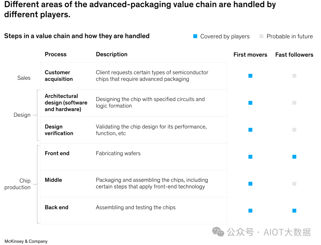
Key players in advanced packaging include logic and memory IDMs, foundries with leading or mature node capabilities, and OSATs. Exhibit 4 shows the capabilities currently handled by first movers and fast followers.
先進封裝的主要參與者包括邏輯和存儲器 IDM、具有領(lǐng)先或成熟節(jié)點能力的代工廠以及 OSAT。圖表 4 顯示了先行者和快速追隨者當(dāng)前所具備的能力。
First movers先行者
First movers have entered the market and are in mass-volume production based on their logic-packaging capabilities. They are actively developing use cases with existing customers and applying cutting-edge advanced-packaging technologies. While these major players are advanced in R&D and manufacturing, they may seek partnerships with followers to stabilize volume as they face rapidly expanding demand.
先行者已經(jīng)進入市場,并基于其邏輯封裝能力進行批量生產(chǎn)。他們正在積極與現(xiàn)有客戶一起開發(fā)用例并應(yīng)用尖端的先進封裝技術(shù)。雖然這些主要參與者在研發(fā)和制造方面處于領(lǐng)先地位,但在面臨快速增長的需求時,他們可能會尋求與追隨者合作以穩(wěn)定產(chǎn)量。
First movers are in mass-volume production based on their logic-packaging capabilities. While these players are advanced in R&D and manufacturing, they may seek partnerships with followers to stabilize volume as they face rapidly expanding demand.
先行者憑借其邏輯封裝能力實現(xiàn)了大批量生產(chǎn)。盡管這些企業(yè)在研發(fā)和制造方面處于領(lǐng)先地位,但在面臨快速增長的需求時,他們可能會尋求與追隨者的合作伙伴關(guān)系來穩(wěn)定產(chǎn)量。
Fast followers快速追隨者
Many fast followers are striving to take a share of the advanced-packaging market but have not mastered the design or manufacturing capabilities or built a sufficient customer base, especially for high-end solutions.
許多快速追隨者正在努力搶占先進封裝市場的份額,但尚未掌握設(shè)計或制造能力,也沒有建立足夠的客戶群,尤其是高端解決方案。
Foundries that have mature node capability but lack advanced packaging could benefit substantially from finding synergies within their current product portfolios. While advanced logic chips with nodes smaller than ten nanometers have the greatest need for advanced packaging, it is critical for fast followers to find opportunities to capture the mature-node market. Some of the areas where advanced packaging can be adapted to enhance the performance of mature-node legacy chips are radio-frequency transceiver chips for network applications, advanced driver-assist systems (ADAS), and infotainment chips for automotive applications.
擁有成熟節(jié)點能力但缺乏先進封裝的代工廠可以從當(dāng)前產(chǎn)品組合中尋找協(xié)同效應(yīng)中獲益匪淺。雖然節(jié)點小于十納米的先進邏輯芯片對先進封裝的需求最大,但對于快速追隨者來說,尋找機會占領(lǐng)成熟節(jié)點市場至關(guān)重要。可以采用先進封裝來增強成熟節(jié)點傳統(tǒng)芯片性能的一些領(lǐng)域包括用于網(wǎng)絡(luò)應(yīng)用的射頻收發(fā)器芯片、高級駕駛員輔助系統(tǒng) (ADAS) 以及用于汽車應(yīng)用的信息娛樂芯片。
Another option is to partner with logic providers to develop design and manufacturing solutions for specific applications that use both mature and leading-edge nodes. The feasibility of this tactic would largely depend on the end-application demand and logic providers’ needs.
另一種選擇是與邏輯提供商合作,為使用成熟和領(lǐng)先節(jié)點的特定應(yīng)用開發(fā)設(shè)計和制造解決方案。這種策略的可行性在很大程度上取決于最終應(yīng)用程序的需求和邏輯提供商的需求。
OSATsOSAT
OSATs’ capabilities in the high-end advanced-packaging market are limited. Rather than trying to compete directly with high-end solutions, they can offer comparatively low-end solutions or seek to collaborate in certain value-chain areas with players capable of high-end advanced packaging. Leading OSATs are actively investing to expand the range of advanced packaging they offer. Some can already handle core and HD-level fan-out packaging, but 2.5-D and 3-D stacking mainly remain in R&D.
OSAT 在高端先進封裝市場的能力有限。他們可以提供相對低端的解決方案,或者尋求在某些價值鏈領(lǐng)域與具有高端先進封裝能力的廠商合作,而不是試圖與高端解決方案直接競爭。領(lǐng)先的 OSAT 正在積極投資以擴大其提供的先進封裝的范圍。有些已經(jīng)可以處理核心和高清級扇出封裝,但 2.5 維和 3 維堆疊主要仍處于研發(fā)階段。
Another option for OSATs is to partner with players capable of 2.5-D and 3-D stacking. While these partners work on core processes—including through-silicon via, RDL lithography, and hybrid bonding—the OSATs could offer solutions for the mid- to back-end processes, including wafer thinning and bumping.
OSAT 的另一個選擇是與能夠進行 2.5-D 和 3-D 堆疊的廠商合作。雖然這些合作伙伴致力于核心工藝(包括硅通孔、RDL 光刻和混合鍵合),但 OSAT 可以為中后端工藝(包括晶圓減薄和凸點)提供解決方案。
Although foundries and IDMs are developing advanced-packaging capabilities, they will likely use advanced packaging only to attract high-end customers that require state-of-the-art technology and, therefore, will not disrupt the entire OSAT business. They are not expected to expand into core and fan-out advanced packaging, given the significant differences in operating margin compared with front-end manufacturing, though they may make the leap into more profitable advanced 2.5-D or 3-D packaging.
盡管代工廠和 IDM 正在開發(fā)先進封裝能力,但他們可能只會使用先進封裝來吸引需要最先進技術(shù)的高端客戶,因此不會擾亂整個 OSAT 業(yè)務(wù)。鑒于運營利潤率與前端制造相比存在顯著差異,預(yù)計它們不會擴展到核心和扇出先進封裝領(lǐng)域,盡管它們可能會進軍利潤更高的先進 2.5-D 或 3-D 封裝領(lǐng)域。
Memory IDMs內(nèi)存 IDM
Logic capability is essential for advanced packaging, but 3-D stacking technology can still present opportunities for memory IDMs, as top players are using it to enhance performance in memory chips that include basic-level logic chips. IDM players can also differentiate themselves by using the technology to customize memory for key clients’ advanced-packaging chips.
邏輯能力對于先進封裝至關(guān)重要,但 3D 堆疊技術(shù)仍然可以為內(nèi)存 IDM 提供機會,因為頂級廠商正在使用它來增強包括基礎(chǔ)級邏輯芯片在內(nèi)的內(nèi)存芯片的性能。IDM廠商還可以利用該技術(shù)為主要客戶的先進封裝芯片定制存儲器,從而使自己脫穎而出。
Another scenario for memory IDMs is to develop logic capabilities, particularly in design or manufacturing, to enable synergies with advanced packaging. This would, however, require substantial investment and a risky leap across the value chain.
內(nèi)存 IDM 的另一個場景是開發(fā)邏輯功能,特別是在設(shè)計或制造方面,以實現(xiàn)與先進封裝的協(xié)同作用。然而,這需要大量投資和跨越價值鏈的冒險跨越。
The advent of advanced packaging has changed the competitive landscape for chip manufacturers. Packaging is no longer a commodity process, and the majors have moved first to make advanced packaging a strategic part of their offerings. Other manufacturers risk being commoditized if they don’t find a way to incorporate advanced packaging into their strategies and offerings. The advanced-packaging market offers many disruptive opportunities, as well as challenges that will likely go beyond business as usual.
先進封裝的出現(xiàn)改變了芯片制造商的競爭格局。包裝不再是一種商品流程,各大公司已首先采取行動,將先進包裝作為其產(chǎn)品的戰(zhàn)略部分。其他制造商如果找不到將先進封裝納入其戰(zhàn)略和產(chǎn)品的方法,則面臨被商品化的風(fēng)險。先進封裝市場提供了許多顛覆性的機遇,也帶來了可能超出常規(guī)業(yè)務(wù)的挑戰(zhàn)。
About the author(s)關(guān)于作者
Ondrej Burkackyis a senior partner in McKinsey’s Munich office, andTaeyoung Kimis a consultant in the Seoul office, whereInji Yeomis an associate partner.
Ondrej Burkacky是麥肯錫慕尼黑辦事處的高級合伙人,Taeyoung Kim是首爾辦事處的顧問,Inji Yeom是麥肯錫辦事處的副合伙人。
在越南投資半導(dǎo)體封裝的機遇與挑戰(zhàn)
越南在半導(dǎo)體產(chǎn)業(yè)尤其是封裝和測試(封測)領(lǐng)域正逐漸成為一個重要的投資目的地。
政府戰(zhàn)略與目標(biāo): 越南政府已經(jīng)制定了一個三階段的半導(dǎo)體產(chǎn)業(yè)路線圖,目標(biāo)是在2030年之前擁有1家芯片制造廠和10家封測廠。這一戰(zhàn)略反映了越南希望成為全球半導(dǎo)體產(chǎn)業(yè)中心之一的雄心。路線圖特別強調(diào)了“C=SET+1”的策略,這里“C”代表芯片,“S”代表專用半導(dǎo)體,“E”代表電子產(chǎn)業(yè),“T”代表人才,而“+1”則指的是越南在半導(dǎo)體供應(yīng)鏈多元化方面的區(qū)位和政策優(yōu)勢。
地理和經(jīng)濟優(yōu)勢: 越南地理位置優(yōu)越,毗鄰中國,這為投資者提供了降低運輸成本和穩(wěn)定供應(yīng)鏈的可能性。此外,越南的勞動力成本相對較低,提供了經(jīng)濟上的吸引力。中國企業(yè)在越南的投資已經(jīng)顯著增加,顯示了強勁的投資趨勢。
地緣政治影響: 中美貿(mào)易戰(zhàn)等地緣政治變化促使在中國設(shè)廠的國際高科技企業(yè)尋找新的生產(chǎn)基地,而越南由于其鄰近中國并且得到美國支持,被視為一個理想的投資地點。這使得越南在半導(dǎo)體封裝領(lǐng)域的投資吸引力進一步增強。
挑戰(zhàn)與考慮: 盡管有諸多優(yōu)勢,越南的投資環(huán)境也面臨一些挑戰(zhàn),如基礎(chǔ)設(shè)施的完善度、法律和政策的透明度以及知識產(chǎn)權(quán)保護等問題。投資者需要權(quán)衡這些因素,確保投資的可持續(xù)性和長期回報。
綜上所述,越南在半導(dǎo)體封裝領(lǐng)域的投資吸引力來自于其戰(zhàn)略規(guī)劃、地理經(jīng)濟優(yōu)勢以及當(dāng)前的國際政治環(huán)境。然而,投資者在進行決策時也應(yīng)全面評估風(fēng)險與挑戰(zhàn)。
-
半導(dǎo)體
+關(guān)注
關(guān)注
334文章
27654瀏覽量
221305 -
3D
+關(guān)注
關(guān)注
9文章
2908瀏覽量
107763 -
2D
+關(guān)注
關(guān)注
0文章
66瀏覽量
15215 -
先進封裝
+關(guān)注
關(guān)注
2文章
422瀏覽量
268
原文標(biāo)題:技術(shù)前沿:半導(dǎo)體先進封裝從2D到3D的關(guān)鍵
文章出處:【微信號:深圳市賽姆烯金科技有限公司,微信公眾號:深圳市賽姆烯金科技有限公司】歡迎添加關(guān)注!文章轉(zhuǎn)載請注明出處。
發(fā)布評論請先 登錄
相關(guān)推薦
如何促使2D和3D視覺檢測的性能成倍提升?
Dialog半導(dǎo)體推出首款2D到3D視頻轉(zhuǎn)換芯片,為智能手機
2D到3D視頻自動轉(zhuǎn)換系統(tǒng)
適用于顯示屏的2D多點觸摸與3D手勢模塊
深度探析英特爾3D封裝技術(shù)
阿里研發(fā)全新3D AI算法,2D圖片搜出3D模型
3d人臉識別和2d人臉識別的區(qū)別
基于神經(jīng)網(wǎng)絡(luò)的2D到3D的機器學(xué)習(xí)
淺談電子集成技術(shù)先進封裝的從2D,3D,4D封裝
【半導(dǎo)光電】先進封裝-從2D,3D到4D封裝


 技術(shù)前沿:半導(dǎo)體先進封裝從2D到3D的關(guān)鍵


評論