


Linear Resistance Meter,線性刻度歐姆表
關鍵字:Linear Resistance Meter
Most analogue multimeters are capable of measuring resistance over quite a wide range of values, but are rather inconvenient in use due to the reverse reading scale which is also non-linear. This can also give poor accuracy due to cramping of the scale that occurs at the high value end of each range. This resistance meter has 5 ranges and it has a forward reading linear scale on each range.The full-scale values of the 5 ranges are 1K, 10K, 100K, 1M &10M respectively and the unit is therefore capable of reasonably accurate measurements from a few tens of ohms to ten Megohms.
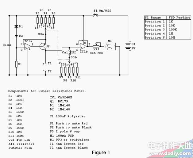
Circuit diagram
The Circuit
Most linear scale resistance meters including the present design, work on the principle that if a resistance is fed from a constant current source the voltage developed across that resistance is proportional to its value. For example, if a 1K resistor is fed from a 1 mA current source from Ohm’s Law it can be calculated that 1 volt will be developed across the resistor (1000 Ohms divided by 0.001 amps = 1 volt). Using the same current and resistance values of 100 ohms & 10K gives voltages of 0.1volts (100 ohms / 0.001amps = 0.1volts) & 10 volts (10000 ohms / 0.001amps = 10 volts).
Thus the voltage developed across the resistor is indeed proportional to its value, and a voltmeter used to measure this voltage can in fact be calibrated in resistance, and will have the desired forward reading linear scale. One slight complication is that the voltmeter must not take a significant current or this will alter the current fed to the test resistor and impair linearity. It is therefore necessary to use a high impedance voltmeter circuit.
The full circuit diagram of the Linear Resistance Meter is given in Figure 1. The constant current generator is based on IC1a and Q1. R1, D1 and D2 form a simple form a simple voltage regulator circuit, which feeds a potential of just over 1.2 volts to the non-inverting input of IC1a. There is 100% negative feedback from the emitter of Q1 to the inverting input of IC1a so that Q1’s emitter is stabilised at the same potential as IC1a’s non-inverting input. In other words it is stabilised a little over 1.2 volts below the positive supply rail potential. S3a gives 5 switched emitter resistances for Q1, and therefore 5 switched emitter currents. S3b provides 5 reference resistors across T1 & T2 via S2 to set full-scale deflection on each range using VR1.
As the emitter and collector currents of a high gain transistor such as a BC179 device used in the Q1 are virtually identical, this also gives 5 switched collector currents. By having 5 output currents, and the current reduced by a factor of 10 each time S3a is moved one step in a clockwise direction, the 5 required measuring ranges are obtained. R2 to R6 must be close tolerance types to ensure good accuracy on all ranges. The high impedance voltmeter section uses IC1b with 100% negative feedback from the output to the inverting input so that there is unity voltage gain from the non-inverting input to the output. The output of IC1b drives a simple voltmeter circuit using VR1 and M1, and the former is adjusted to give the correct full-scale resistance values.
The CA3240E device used for IC1 is a dual op-amp having a MOS input stage and a class A output stage. These enable the device to operate with the inputs and outputs right down to the negative supply rail voltage. This is a very helpful feature in many circuits, including the present one as it enables a single supply rail to be used where a dual balanced supply would otherwise be needed. In many applications the negative supply is needed simply in order to permit the output of the op-amp to reach the 0volt rail. In applications of this type the CA3240E device normally enables the negative supply to be dispensed with.
As the CA3240E has a MOS input stage for each section the input impedance is very high (about 1.5 million Megohms!) and obviously no significant input current flows into the device. This, together with the high quality of the constant current source, and the practically non-existent distortion through IC1b due to the high feedback level gives this circuit excellent linearity.
With no resistor connected across T1 & T2 M1 will be taken beyond full-scale deflection and overloaded by about 100 or 200%. This is unlikely to damage the meter, but to be on the safe side a push-to-test on/off switch (S1) is used. Thus the power is only applied to the circuit when a test resistor is connected to the unit, and prolonged meter overloads are thus avoided.
A small (PP3 size) 9 volt battery is a suitable power source for this project which has a current consumption of around 5mA and does not require a stabilised supply.
Photos showing inside and outside of the completed Linear Resistance Meter.
Author: Dave Elliott
Email: portagepal@tiscali.co.uk
Email: portagepal@tiscali.co.uk
聲明:本文內容及配圖由入駐作者撰寫或者入駐合作網站授權轉載。文章觀點僅代表作者本人,不代表電子發燒友網立場。文章及其配圖僅供工程師學習之用,如有內容侵權或者其他違規問題,請聯系本站處理。
舉報投訴
發布評論請先 登錄
相關推薦
熱點推薦
線性電機(linear motor)介紹
線性馬達一般指線性電機線性馬達是一種將電能直接轉換成直線運動機械能,而不需要任何中間轉換機構的傳動裝置。它可以看成是一臺旋轉電機按徑向剖開,并展成平面而成。直線電機也稱線性電機,
鼎陽科技推出新一代精密源表SMM3000X系列
編程及測量分辨率,最大采集速率100,000 points/s。支持四象限操作,能夠同時采集和測量信號,實現對DUT的源-測量循環。既可作為恒壓源、恒流源、電壓表、電流表和歐姆表,還可以作為脈沖發生器、波形發生器,是測試半導體和

ADGS2414D: 0.56 Ω On Resistance High Density Octal SPST Switch Data Sheet adi
資料,ADGS2414D: 0.56 Ω On Resistance High Density Octal SPST Switch Data Sheet真值表,ADGS2414D: 0.56
發表于 01-15 18:51

TPL5010的Digital conversion of external resistance (Rext)功耗是怎么計算的?
Datasheet的7.5中有關于Digital conversion of external resistance (Rext)的功耗,
請問,這個功耗應該怎么理解,和總體功耗有什么關系?
發表于 11-08 08:09
歐姆定律與電路分析技巧
歐姆定律是電路分析中的基石,它描述了電流、電壓和電阻之間的基本關系。在進行電路分析時,掌握一些基于歐姆定律的技巧可以幫助我們更有效地理解和解決問題。以下是一些關于歐姆定律與電路分析技巧的討論: 一
歐姆定律的實際應用實例
歐姆定律是電氣工程和物理學中的一個基本定律,它描述了電流、電壓和電阻之間的關系。這個定律由德國物理學家喬治·西蒙·歐姆在1827年首次提出,其公式為 V = IR,其中 V 代表電壓(伏特),I
歐姆定律的常見誤區
歐姆定律是電磁學中的一個基本定律,它描述了電流、電壓和電阻之間的關系。這個定律以德國物理學家喬治·西蒙·歐姆的名字命名,他在1827年首次發表了這一定律。盡管歐姆定律在中學物理課程中廣泛教授,但仍然
75歐姆N頭特點及應用介紹
德索工程師說道75歐姆N頭,即75歐姆的N型連接器,是N系列射頻同軸連接器的一種,具有獨特的特性和廣泛的應用場景。以下是對75歐姆N頭的特點及應用進行的詳細介紹。
阻抗匹配:75歐姆

請問TAS3251的DAC output可以用來接VM meter嗎?
請問 TAS3251 的 DAC output 可以用來接 VM meter 嗎?
還是有哪些訊號可以搭接VM meter
謝謝
發表于 10-14 06:55
零歐姆電阻的作用和使用技巧
零歐姆電阻,又稱為跨接電阻器,是一種特殊用途的電阻。盡管名為“零歐姆”,但實際上其電阻值并非真正為零,而是非常小,在電路中可以近似看作零歐姆。它在電路設計中具有多種重要作用和使用技巧,以下是對零
電流計改裝成電壓表時刻度怎么刻
將電流計改裝成電壓表時,刻度的刻畫是一個關鍵步驟,它確保了改裝后的電壓表能夠準確地測量電壓。以下是步驟和原理: 一、改裝原理 電流計改裝成電壓表的主要原理是通過串聯一個電阻(稱為分壓電
75歐姆同軸線纜解析
同軸線纜中阻抗一般分為50歐姆和75歐姆,由于75歐姆線纜用途較為單一,在整個同軸線纜中,50歐姆占主導優勢。雖然75歐姆同軸線纜類型較少,

萬用表測電阻黑表筆接哪個極
萬用表測電阻時,黑表筆接的極性與萬用表的類型(指針式或數字式)有關。 指針式萬用表 對于指針式萬用表,在測量電阻時,黑表筆連接的是歐姆表內部
歐姆表倍率與內阻的關系
歐姆表是一種用于測量電阻的便攜式電子儀器,廣泛應用于電子、電氣和通信領域。它的原理基于歐姆定律,即電壓與電流成正比,而電阻則是電壓與電流的比值。在實際應用中,歐姆表的倍率是一個關鍵參數,它直接影響
什么定律體現了線性電路元件上電壓 歐姆定律在實際電路中的應用
線性電路元件上的電壓與電流之間的關系遵循歐姆定律。 1. 歐姆定律的基本概念 歐姆定律是描述電阻、電壓和電流之間關系的定律。在最簡單的形式中,歐姆


 工商網監
工商網監

評論