 電子發燒友App


NXP公司的LPC2930是集成了ARM968E-S CPU核和兩個TCM區塊的MCU,工作頻率高達125MHz,并具有全速USB 2.0 Host/OTG/Device控制器,CAN和LIN,56 kB SRAM,外接存儲器接口,三個10位ADC和多種串行接口,可廣泛應用在消費電子,工業和通信市場。本文介紹了LPC2930主要特性和優勢,整體方框圖和各種功能的方框圖,包括時鐘區框圖,調制和取樣控制子系統(MSCSS)方框圖,ADC方框圖,PWM方框圖,PCRSS方框圖,CGU0和CGU1方框圖,時鐘發生架構圖和PLL方框圖以及自供電USB接口框圖與USB OTG端口配置圖。
The LPC2930 combine an ARM968E-S CPU core with two integrated TCM blocks operating at frequencies of up to 125 MHz, Full-speed USB 2.0 Host/OTG/Device controller, CAN and LIN, 56 kB SRAM, external memory interface, three 10-bit ADCs, and multiple serial and parallel interfaces in a single chip targeted at consumer, industrial, and communication markets. To optimize system power consumption, the LPC2930 has a very flexible Clock Generation Unit (CGU) that provides dynamic clock gating and scaling.
LPC2930主要特性和優勢:
ARM968E-S processor running at frequencies of up to 125 MHz maximum.
Multilayer AHB system bus at 125 MHz with four separate layers.
On-chip memory:
Two Tightly Coupled Memories (TCM), 32 kB Instruction TCM (ITCM), 32 kB Data TCM (DTCM).
Two separate internal Static RAM (SRAM) instances; 32 kB SRAM and 16 kB SRAM.
8 kB ETB SRAM, also usable for code execution and data.
Dual-master, eight-channel GPDMA controller on the AHB multilayer matrix which can be used with the SPI interfaces and the UARTs, as well as for memory-to-memory transfers including the TCM memories.
External Static Memory Controller (SMC) with eight memory banks; up to 32-bit data bus; up to 24-bit address bus.
Serial interfaces:
USB 2.0 full-speed Host/OTG/Device controller with dedicated DMA controller and on-chip device PHY.
Two-channel CAN controller supporting FullCAN and extensive message filtering
Two LIN master controllers with full hardware support for LIN communication. The LIN interface can be configured as UART to provide two additional UART interfaces.
Two 550 UARTs with 16-byte Tx and Rx FIFO depths, DMA support, modem control, and RS-485/EIA-485 (9-bit) support.
Three full-duplex Q-SPIs with four slave-select lines; 16 bits wide; 8 locations deep;Tx FIFO and Rx FIFO.
Two I2C-bus interfaces.
Other peripherals:
One 10-bit ADC with 5.0 V measurement range and eight input channels with conversion times as low as 2.44 μs per channel.
Two 10-bit ADCs, 8-channels each, with 3.3 V measurement range provide an additional 16 analog inputs with conversion times as low as 2.44 μs per channel.Each channel provides a compare function to minimize interrupts.
Multiple trigger-start option for all ADCs: timer, PWM, other ADC, and external signal input.
Four 32-bit timers each containing four capture-and-compare registers linked to I/Os.
Four six-channel PWMs (Pulse-Width Modulators) with capture and trap functionality.
Two dedicated 32-bit timers to schedule and synchronize PWM and ADC.
Quadrature encoder interface that can monitor one external quadrature encoder.
32-bit watchdog with timer change protection, running on safe clock.
Up to 152 general-purpose I/O pins with programmable pull-up, pull-down, or bus keeper.
Vectored Interrupt Controller (VIC) with 16 priority levels.
Up to 22 level-sensitive external interrupt pins, including USB, CAN and LIN wake-up features.
Processor wake-up from power-down via external interrupt pins, CAN, or LIN activity.
Configurable clock-out pin for driving external system clocks.
Flexible Reset Generator Unit (RGU) able to control resets of individual modules.
Flexible Clock-Generation Unit (CGU) able to control clock frequency of individual modules:
On-chip very low-power ring oscillator; fixed frequency of 0.4 MHz; always on to provide a Safe_Clock source for system monitoring.
On-chip crystal oscillator with a recommended operating range from 10 MHz to 25 MHz. PLL input range 10 MHz to 25 MHz.
On-chip PLL allows CPU operation up to a maximum CPU rate of 125 MHz.
Generation of up to 11 base clocks.
Seven fractional dividers.
Second, dedicated CGU with its own PLL generates USB clocks and a configurable clock output.
Highly configurable system Power Management Unit (PMU):
clock control of individual modules.
allows minimization of system operating power consumption in any configuration.
Standard ARM test and debug interface with real-time in-circuit emulator.
Boundary-scan test supported.
ETM/ETB debug functions with 8 kB of dedicated SRAM also accessible for application code and data storage.
Dual power supply:
CPU operating voltage: 1.8 V ± 5 %.
I/O operating voltage: 2.7 V to 3.6 V; inputs tolerant up to 5.5 V.
208-pin LQFP package.
?40℃pplication ?to +85℃ ambient operating temperature range.
圖1。LPC2930方框圖
圖2。LPC2930時鐘區框圖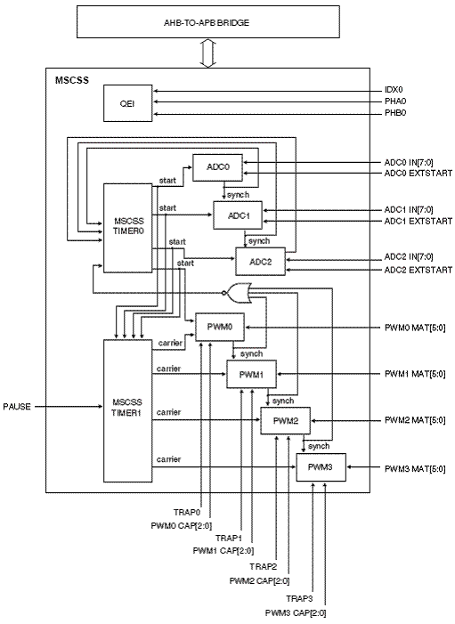
圖3。LPC2930調制和取樣控制子系統(MSCSS)方框圖
圖4。LPC2930 ADC方框圖
圖5。LPC2930 PWM方框圖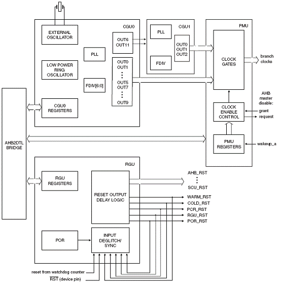
圖6。LPC2930 PCRSS方框圖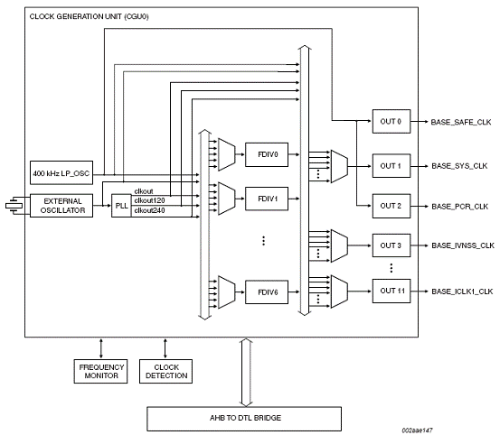
圖7。LPC2930 CGU0方框圖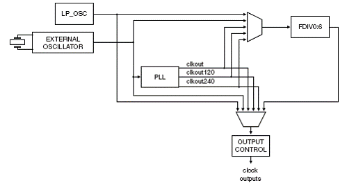
圖8。LPC2930時鐘發生架構圖
圖9。LPC2930 PLL方框圖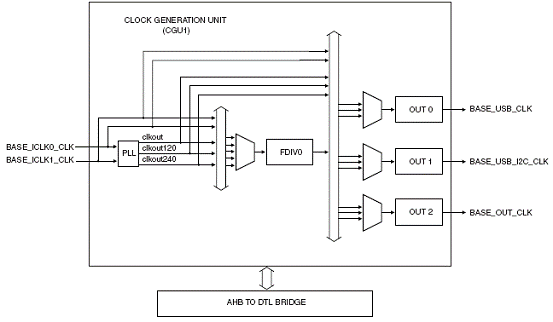
圖10。LPC2930 CGU1方框圖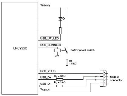
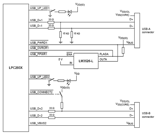
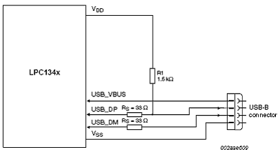
圖11。LPC2930 自供電USB接口框圖
圖12。LPC2930 總線供電USB接口框圖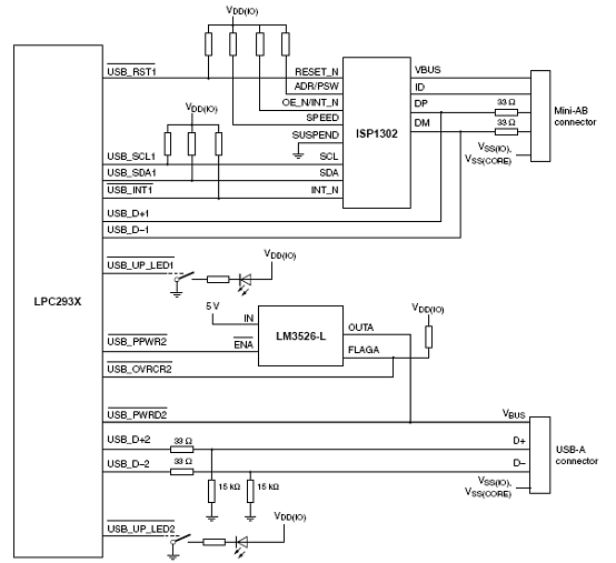
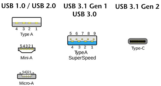
圖13。LPC2930 USB端口配置圖:USB端口1 OTG雙規設備,USB端口2主機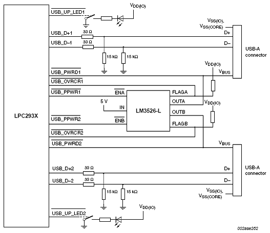
圖13。LPC2930 USB OTG端口配置圖:USB端口1 主機,USB端口2主機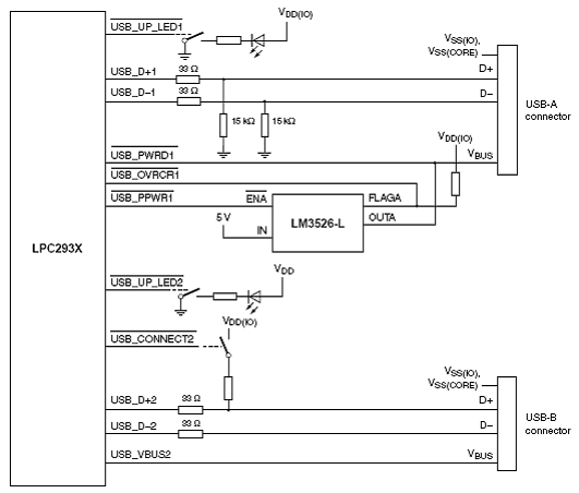
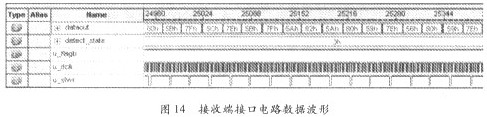
圖14。LPC2930 USB OTG端口配置圖:USB端口2 設備,USB端口1主機
基于LPC2930設計的高速USB-OTG接口方案
- US(46135)
- LPC2930(6687)


相關推薦
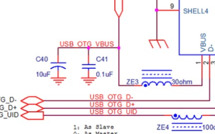
USB OTG Vbus電源框圖及應用方案
到智能手機以及從相機到打印機之間的數據傳輸需求也隨之增加。 USB On-the-Go(OTG)是使設備能夠充當主設備或從設備的規范。USB OTG可廣泛應用于PC、智能手機、ePOS(電子銷售點)和移動電源。主設備或從設備的角色可以根據協議進行改變。數據可
2018-03-09 09:21:13 17788
17788
17788
基于TF32A09系列芯片的高速數據流加密的解決方案
高速數據流加密轉接器具有2個USB 2.0高速(480Mb/s)接口(OTG)和內置高速加密算法(如SM1)。其中USB_Host接口和傳統的移動存儲設備相接、USB_Device接口和PC機相接
2019-01-04 08:14:005715
5715
OTG硬件檢測電路
1. OTG接口與轉換器 OTG是"On The Go"的英文縮寫,字面上可以理解為“安上即可用”。USB傳輸是主從結構,一切USB傳輸都有Host發起。比如在開發板上可以插入
2023-07-11 08:40:46868
868
LPC2930
LPC2930 - ARM9 flashless microcontroller with CAN, LIN, and USB - NXP Semiconductors
2022-11-04 17:22:44
LPC2930FBD208
LPC2930FBD208 - ARM9 flashless microcontroller with CAN, LIN, and USB - NXP Semiconductors
2022-11-04 17:22:44
USB-OTG是否需要連接Vbussx才能用作USB大容量存儲器呢?
了評估板與我的定制板的 shematc 比較。此外,USB-ORG 作為 DFU 設備在工程模式下工作——所以我猜焊接和 USB 引出線是正確的。圖1。USB-OTG2.Pic的自定義電路板原理圖。USB-OTG 的評估板原理圖。
2022-12-14 07:56:39
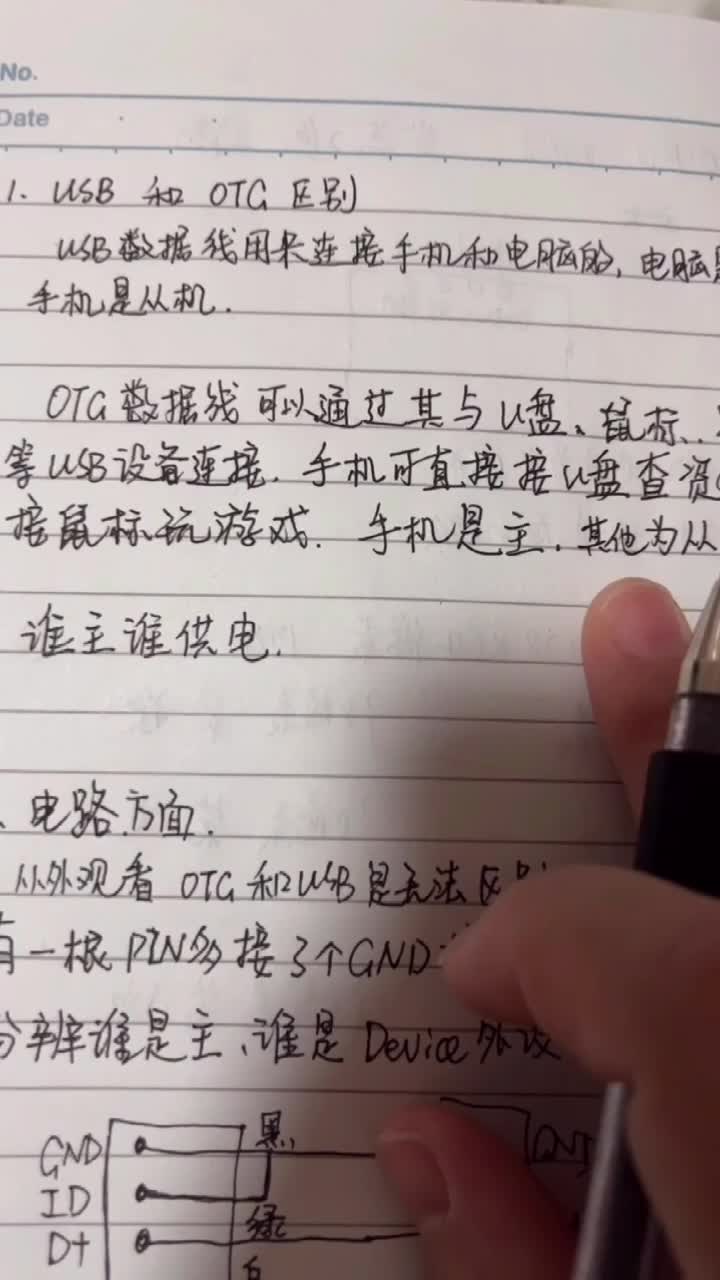
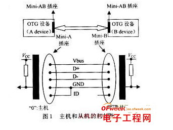
USB OTG原理+ ID 檢測原理
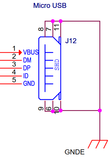
。也就是說,手機既可以做外設,又可以做主機來傳送數據,可用電纜的連接方式來決定初始角色(由ID線的狀態來決定)。USB OTG接口中有5條線: 2條用來傳送數據(D+ 、D-);1條是電源線(VBUS
2015-02-10 11:19:47
USB接口易損壞的解決方案
該問題由某客戶提出,發生在 STM32F205VCT6 器件上。據其工程師講述:為了實現產品的設計中使用STM32 的 USB OTG 接口,作為其產品的一個通用 USB 接口來用。在其產品小批量試產后,發現STM32的 USB OTG 接口在其產品的使用過程中易損壞。
2023-09-08 06:13:11
USB接口的 MP3/WMA播放方案OTG13T
USB接口的 MP3/WMA播放方案OTG13T 板載USB接口,支持所有市售
2010-03-12 11:20:28
USB高速物理層不工作怎么解決?
數據。如果禁用 OTG 的內部 DMA,全速 USB 設備工作正常,但高速設備無法在枚舉時傳輸設置命令。如果啟用 OTG 的內部 DMA,則所有全速和高速設備都無法枚舉。有沒有成功案例?
2023-01-05 08:43:05


 工商網監
工商網監
評論