Many articles have been written about the building blocks in a typical data acquisition system, but few address the entire system, from analog input to PC display. To cover all the problems encountered in designing a complete data acquisition system, the engineer might have to amass ten articles.
The following application note describes the design of a PC-based, 14-bit data acquisition system. It takes a system approach, includes all the necessary building blocks: analog, digital, hardware, and software. It discusses each step, testing systems separately before integrating them, and detailing pitfalls learned along the way.
The Design Specification
The task: Design a power meter based on a 14-bit simultaneous-sampling ADC with on-chip RAM (MAX125).The need for a power meter is apparent to anyone who has tried measuring the input and output characteristics of a DC-DC converter using conventional instruments. The design allows users to perform load measurements on the device under test without connecting an endless spaghetti-mass of test leads. Figure 1 shows the completed power meter display on a personal computer (PC) monitor.
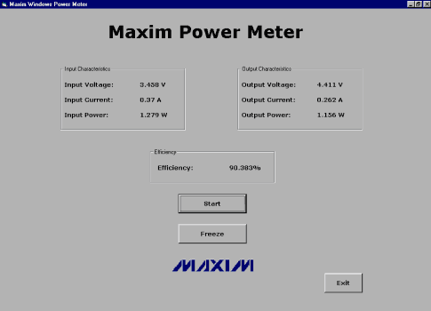
Figure 1. Windows PC output with example readout.
To cater for boost, buck, and linear implementations, the measurement range was chosen as 30V for both input and output. Most quality DC-DC converters operate at 100kHz or higher. The system's frequency response should therefore be higher than 100kHz, but a slower response is also acceptable because the switching waveforms are reasonably repetitive.
The system's 14-bit resolution was not of prime importance in the design stage, because measurements to within 0.1% (10 bits) are perfectly adequate for most power-meter applications. Once digitized, the results are uploaded via an RS-232 interface and displayed on a PC screen, with an update rate of once per second (like most multimeters). Once data arrives at the RS-232 port, the power of the PC can be unleashed upon it. The full circuit diagram (Figure 2) will be discussed in sections:
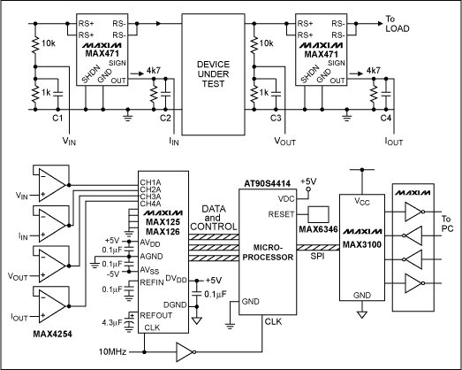
Figure 2. Circuit diagram.
Analog Front End
A precision resistive divider allows accurate voltage measurements up to 30V. The ORNA10-1 from Vishay Thin Film is a trimmed resistor network comprising two 1kΩ and two 10kΩ values. The ratiometric accuracy of these four resistors is 0.05%, and so provides a precision fraction (1/11) of the applied voltage. The MAX125's fault-protected input has a range of ±5V, which allows a degree of safety under fault conditions and plenty of headroom for input and output voltage measurements.Input and output currents are measured using the precision current amplifier MAX471. This device measures the voltage across an internal 30mΩ resistor, and delivers an output current whose amplitude equals 500uA per ampere of high-side current. Thus, the value of an external resistor scales the output voltage, and suitable resolution is achieved in this case by selecting a value of 4.7kΩ.
The MAX125's wide input capability and fault-protection circuitry give it a lower input impedance than that of equivalent competitive devices, so the four readings are buffered before entering the ADC. Unity-gain buffer stages are taken from the MAX4254 quad precision op amp, whose input offset voltages (70uV) are lower than the system resolution.
The MAX125 inputs are buffered mainly to overcome their low input impedance, but driving an ADC from low impedance is always good practice even when the converter has a high input impedance. Because sample/hold circuitry is normally placed right at the ADC input, the buffer provides the necessary drive for charging the sample/hold capacitor in an acceptable time. To get an idea of how low the source impedance has to be, consider a simple calculation of RC time constant. The input capacitor charges according to
vcap = vin (1-e-t/CR),
where C is the sampling capacitor, R is the source resistance, and Vin is the voltage applied to the RC circuit. The difference in voltage between Vin and Vcap is:
vin - vcap = vin e-t/CR
Therefore, given the value of the sample and hold capacitor (normally 10-30pF), the charging time of the capacitor, and the error voltage that can be tolerated (1/2 LSB), one can calculate the maximum allowable signal-source resistance that will charge the capacitor in a given time.
The input buffer can also serve as a filter for removing unwanted signals. Because the ADC is a sampling system, its output has spectral symmetry centered about half the sampling frequency. Thus, signals greater than half the sampling frequency cannot be distinguished from signals less than half the sampling frequency. With a 10kHz sampling frequency, for example, the ADC is not able to distinguish between a 4kHz and a 6kHz input, because both are symmetrical about half the sampling frequency (5kHz). Though too detailed for the scope of this article, this effect (aliasing) and the theorem that describes it (Nyquist's theorem) are described in many papers and books.
An "anti-aliasing filter" removes these unwanted frequencies. The effect of aliasing can be quite subtle if you consider the frequency spectrum of any signal that is not purely sinusoidal. A non-sinewave by definition has harmonics, and these higher harmonics translate downward to cause errors at the lower frequencies. Again, unless the input signal frequency range is definitely known, a combination buffer and anti-aliasing filter is always good design practice.
Minimal filtering is required because the system in question takes only spot readings. For higher sampling frequencies, a simple lowpass filter using components C1, C2, C3, and C4 provides signal rolloff ahead of the ADC input. These components also serve to average out the readings taken by the ADC, and they effectively remove ripple from the input and output power measurements.
Digitization
The MAX125 is a self-contained, simultaneous-sampling, successive-approximation data-acquisition system with on-chip RAM. It samples two sets of four signals using 2x4 sample/hold amplifiers, which are then digitized sequentially by a single ADC block. The results are stored in RAM and read out sequentially on the parallel data bus under processor control.The MAX125 also includes a voltage reference whose spurious-free dynamic range (SFDR) is suitable for many high-resolution DSP applications. (The internal reference can be overridden by an external system reference.) The MAX125 also exhibits good INL (the maximum deviation of real from theoretical ADC output), good DNL (the deviation of real from theoretical ADC step magnitude) and monotonicity to 13 bits (an output code that increases or remains unchanged in response to an increasing analog input). To enable efficient use of the microprocessor, the MAX125 provides a push-pull interrupt output indicating when the conversion has finished.
An internal buffer allows use of either the internal or an external reference. As for the analog input, the reference input should be driven from a low-impedance source. This applies especially for ADCs that employ a successive-approximation register (SAR), because the reference voltage feeds directly into the DAC's R-2R ladder. As the DAC's input code changes, the input impedance of the reference input also changes, thereby modulating the reference voltage. Fortunately, the MAX125's internal buffer eliminates this concern.
For this design, the internal reference was overridden by an external, precision, low-dropout, low-drift 2.5V voltage reference (MAX873A). Although its use (vs. the internal reference) provided no noticable change in results, the MAX873A offers better initial accuracy and drift.
Gaining an idea of the drift specification (in ppm/°C) needed for any digitisation system is straightforward. First, define the system's operating temperature range. For this application, assume a normal lab temperature range of 30°C. Next, decide on the maximum drift (in volts) that can be tolerated (normally 1/2 to 1 LSB) over the temperature range, and hence the drift in V/°C. To normalise this drift value to ppm/°C, divide by the reference voltage and multiply by 106. The result is normally about 2ppm/°C for a 14-bit system, 10ppm/°C for a 12-bit system, and 30ppm/°C for a 10 bit system. These figures change according to the allowable temperature span and total reference drift.
The MAX125 is driven by an Atmel AVR processor (AT90S4414), and both are clocked at the same frequency (10MHz) derived from an oscillator module. The program was written in assembly language, with a single instruction toggling each data line to reflect timing diagrams in the MAX125 datasheet. The program is divided into subroutines for easier understanding, and most lines are commented for the same purpose.2
At startup or power-on-reset, the MAX125 is configured using the bidirectional data pins D3-D0. Setting these pins to 0011 and strobing WR low sets the ADC's mode of operation to receive inputs from all four channels of MUX A. Once this is established, the microprocessor ports are reconfigured as inputs to receive data from the ADC.
When CONVST is pulsed low, the processor waits for an interrupt signal from the MAX125. It then reads out the conversion of channel 1 and sends the result (via the MAX3100 UART and the MAX202E) to the PC's RS-232 port. Each conversion includes 16 bits of data, so each result requires two RS-232 write cycles. Because the ADC stores the conversions from channels 2-4, the time taken to transmit the RS-232 data can be fairly leisurely. When the data from channel 1 has been sent, the process is repeated for Channels 2-4.
Noise pickup was noted on unused data pins of the microprocessor bus (a 16-bit-wide bus with only 14 data lines). If these unused pins are configured as inputs, the noise faithfully masquerades as intermittent data. Fortunately, however, a simple software AND function filters out the induced noise and they say digital filtering is tough! As an alternative, you can configure the unused ports as outputs.
The above code works perfectly, but establishing correct circuit performance can prove difficult. The interrupt pulse from the μC comes and goes so fast (in 1μs) that only a storage oscilloscope can detect it. If a suitable oscilloscope is not available, you can insert a delay routine immediately after the CONVST line has been set HIGH to enable a more leisurely viewing of the interrupt signal.
The PC Interface
The key component interfacing the microprocessor to the PC is the serially addressed UART (MAX3100). It takes input from the microprocessor via its 4-wire SPI?/Microwire bus3, and converts this data to the format used by most RS-232 compatible devices. An industry-standard, micropower 2TX/2RX transceiver (MAX202E) implements the level translation.This UART, which has hardware and software shutdown modes and comes in a tiny QSOP package, is ideally suited for low-power portable appliances. For hazardous environments, its interface also allows IrDA communication by attachment of suitable optical devices. Other features (not required in this application) include a receive buffer and an interrupt flag to give status information on the transmit and receive registers.
A software-based SPI routine is implemented for exporting the code to microprocessors lacking a built-in SPI bus. The code shows that this is a trivial task, and comments guide the uninitiated through the clock cycles of the SPI bus. If a dedicated SPI port is used, it is worth noting that the MAX3100's serial clock line (SCLK) must start in the LOW state when CS is asserted. If this requirement presents a problem, you should cycle the SCLK line before entering the SPI routine.
Note the time required for RS-232 data to transmit. At 9600 baud, it takes more than one millisecond to transmit eight bits of data together with the start and stop bits. This is obvious in hindsight, but it can give the designer hours of undeserved enjoyment not only in wondering why data is not reaching the PC correctly, but also in illustrating the difference in operating speeds of the microprocessor and the RS-232 link. A simple 10ms delay inserted in the code allows data transmission and processing at the PC end. Note also that the RS-232 spec does not detail the signal protocol (start and stop bits, etc.); just the voltage levels, slew rate, and connector details. The MAX3100 and MAX202E, however, handle all the standards for making data compliant with RS-232, and in a protocol expected by the PC.
The Windows? Interface
The Windows program was written in Visual Basic Version 6. It takes readings from the RS-232 port using the MSComm function, configured to accept text, and converts this data to ASCII. It also translates each 16-bit data block back to the voltage and current measurements obtained from analog-sensing circuitry that precedes the ADC input. From these results, the input power, output power, and efficiency are calculated and displayed on the PC screen, rounded to three decimal places. In addition, the system can "freeze" the results if they need to be logged.The measured efficiency figures were far from consistent. This was accounted for by noticing ripple on the current and voltage waveforms. The 4.7kΩ resistors were bypassed with 10nF capacitors to reduce the current-ripple readings, but the resistive-divider networks measuring voltage were left unbypassed. Thus, the measured ripple (20mV on the input and 100mV on the output) accounted for the ±3% variation in efficiency measurements.
As results are read into the PC, missing data produces incorrect readings on the PC screen. The time intervals between arriving packets of data were therefore measured. If any interval exceeded 0.5 seconds, the PC counter was reset in anticipation of the first character in the subsequent data packet.
Results
The device under test (DUT) was the MAX1705, a boost DC-DC converter configured in PWM mode. Loads were applied to the evaluation kit, and the results taken by freezing the MAX125 PC program and reading values from the screen. The results were then confirmed using the (now obsolete) digital multimeter, and compared with the expected efficiency as given by graphs in the datasheet:Table 1.
| Load/Ω | Vin/V | Iin/A | Vout/V | Iout/A | Efficiency/% | (exp. Eff/%) |
| 16.4 | 3.384 | 0.377 | 4.485 | 0.262 | 92.09 | 95 |
| 50 | 3.451 | 0.123 | 4.478 | 0.086 | 90.8 | 92 |
| 100 | 3.498 | 0.064 | 4.471 | 0.042 | 83.9 | 83 |
| 390 | 3.545 | 0.021 | 4.485 | 0.009 | 54.054 | 56 |
Calibration, Errors and Tweaks
Though digital purists may argue differently, the analog board layout must be impeccable to obtain the best circuit performance. All power rails to the analog ICs should be thick, and decoupled to ground with capacitors physically close to the devices: at least 1uF (tantalum) in parallel with 100nF (ceramic). A good ground plane should be included, especially around the MAX471, because high frequency, high amplitude currents occupy that territory. The 4.7kΩ resistors on the MAX471 should be precision types with low inductance, because any tolerance on these components directly affects the results. All analog PCB tracks should be as short as possible and far away from digital lines. The MAX125 reference amplifier should be decoupled at input and output, close to the IC. Ideally, the board should incorporate separate analog and digital ground planes, connected at a single point.It was observed that the 10MHz clock appears in unexpected places, so if this signal is to be routed across the pc board it should be physically remote from analog inputs, especially the resistor networks and with a ground track in between. To further minimize noise radiation, this signal can be filtered to remove clock harmonics and reconstituted using a simple digital gate placed close to the processor and ADC. A '74HC00 works well for this purpose.
A number of factors should be considered to obtain absolute dc accuracy. The MAX873A reference offers excellent drift specifications, for example, but its initial accuracy (±1.5mV) gives a ±10LSB error in 14-bit systems. This error can be trimmed by connecting a trim pot between the output trim pin and ground. It is advisable to switch the reference voltage across both the input and output resistive dividers, and read the input signal to the ADC. From this reading, you can determine errors in the resistive divider chain and implement a software offset.
To accurately calibrate the current-sense amplifiers, you must take ADC readings while applying a current source to the input and output, thus obtaining the error in the current amplifier and output resistor. This current source should be set at the minimum expected current reading, because the MAX471 dominant error at low currents is due to input offset voltage contributed by the internal op amps.
 電子發(fā)燒友App






評(píng)論