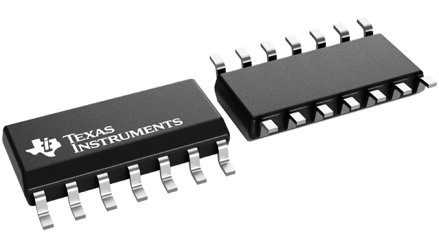
| Number of channels (#) | 4 |
| Total supply voltage (Max) (+5V=5, +/-5V=10) | 16 |
| Total supply voltage (Min) (+5V=5, +/-5V=10) | 2.7 |
| Vos (offset voltage @ 25 C) (Max) (mV) | 0.85 |
| GBW (Typ) (MHz) | 0.2 |
| Features | High Cload Drive |
| Slew rate (Typ) (V/us) | 0.12 |
| Rail-to-rail | In to V-, Out |
| Offset drift (Typ) (uV/C) | 0.5 |
| Iq per channel (Typ) (mA) | 0.03375 |
| Vn at 1 kHz (Typ) (nV/rtHz) | 19 |
| CMRR (Typ) (dB) | 75 |
| Rating | HiRel Enhanced Product |
| Operating temperature range (C) | -40 to 125 |
| Input bias current (Max) (pA) | 60 |
| Output current (Typ) (mA) | 8 |
| Architecture | CMOS |
| THD + N @ 1 kHz (Typ) (%) | 0.2 |
- Controlled Baseline
- One Assembly/Test Site, One Fabrication Site
- Extended Temperature Performance of –40°C to 125°C
- Enhanced Diminishing Manufacturing Sources (DMS) Support
- Enhanced Product-Change Notification
- Qualification Pedigree

- ESD Protection Exceeds 2000 V Per MIL-STD-883, Method 3015; Exceeds 150 V (TLV2252/52A) and 100 V (TLV2254/54A) Using Machine Model (C = 200 pF, R = 0)
- Output Swing Includes Both Supply Rails
- Low Noise . . . 19 nV/
 Hz\ Typ at f = 1 kHz
 - Low Input Bias Current . . . 1 pA Typ
- Fully Specified for Both Single-Supply and Split-Supply Operation
- Very Low Power . . . 34 μA Per Channel Typ
- Common-Mode Input Voltage Range Includes Negative Rail
- Low Input Offset Voltage: 850 μV Max at TA = 25°C
- Wide Supply Voltage Range: 2.7 V to 16 V
- Macromodel Included
 Component qualification in accordance with JEDEC and industry standards to ensure reliable operation over an extended temperature range. This includes, but is not limited to, Highly Accelerated Stress Test (HAST) or biased 85/85, temperature cycle, autoclave or unbiased HAST, electromigration, bond intermetallic life, and mold compound life. Such qualification testing should not be viewed as justifying use of this component beyond specified performance and environmental limits.
Advanced LinCMOS is a trademark of Texas Instruments.
The TLV2252 and TLV2254 are dual and quadruple low-voltage operational amplifiers from Texas Instruments. Both devices exhibit rail-to-rail output performance for increased dynamic range in single- or split-supply applications. The TLV225x family consumes only 34 μA of supply current per channel. This micropower operation makes them good choices for battery-powered applications. This family is fully characterized at 3 V and 5 V and is optimized for low-voltage applications. The noise performance has been dramatically improved over previous generations of CMOS amplifiers. The TLV225x has a noise level of 19 nV/ Hz at 1kHz, four times lower than competitive micropower solutions.
The TLV225x, exhibiting high input impedance and low noise, are excellent for small-signal conditioning for high-impedance sources, such as piezoelectric transducers. Because of the micropower dissipation levels combined with 3-V operation, these devices work well in hand-held monitoring and remote-sensing applications. In addition, the rail-to-rail output feature with single or split supplies makes this family a great choice when interfacing with analog-to-digital converters (ADCs). For precision applications, the TLV225xA family is available and has a maximum input offset voltage of 850 μV.
The TLV2252/22544 also make great upgrades to the TLV2322/2424 in standard designs. They offer increased output dynamic range, lower noise voltage, and lower input offset voltage. This enhanced feature set allows them to be used in a wider range of applications. For applications that require higher output drive and wider input voltage range, see the TLV2432 and TLV2442 devices. If your design requires single amplifiers, please see the TLV2211/21/31 family. These devices are single rail-to-rail operational amplifiers in the SOT-23 package. Their small size and low power consumption, make them ideal for high density, battery-powered equipment.


