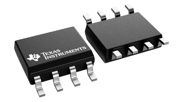
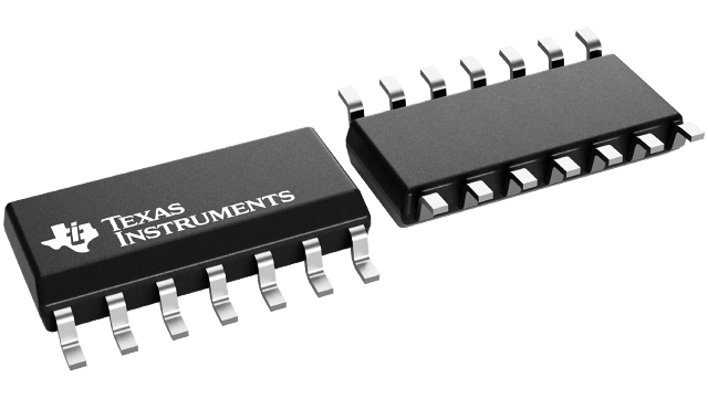
| Architecture | Current FB |
| Number of channels (#) | 2 |
| Total supply voltage (Min) (+5V=5, +/-5V=10) | 4 |
| Total supply voltage (Max) (+5V=5, +/-5V=10) | 12 |
| GBW (Typ) (MHz) | 280 |
| BW @ Acl (MHz) | 280 |
| Acl, min spec gain (V/V) | 1 |
| Slew rate (Typ) (V/us) | 2100 |
| Vn at flatband (Typ) (nV/rtHz) | 1.7 |
| Vn at 1 kHz (Typ) (nV/rtHz) | 1.7 |
| Iq per channel (Typ) (mA) | 5.1 |
| Vos (offset voltage @ 25 C) (Max) (mV) | 3 |
| Rail-to-rail | No |
| Features | Shutdown |
| Rating | Catalog |
| Operating temperature range (C) | -40 to 85 |
| CMRR (Typ) (dB) | 56 |
| Input bias current (Max) (pA) | 35000000 |
| Offset drift (Typ) (uV/C) | 20 |
| Output current (Typ) (mA) | 190 |
| 2nd harmonic (dBc) | 70 |
| 3rd harmonic (dBc) | 74 |
| Frequency of harmonic distortion measurement (MHz) | 5 |
- FLEXIBLE SUPPLY RANGE:
???+5V to +12V Single Supply
???±2.5V to ±6V Dual Supply - WIDEBAND +5V OPERATION: 190MHz (G =+2)
- UNITY-GAIN STABLE: 280MHz (G =1)
- HIGH OUTPUT CURRENT: 190mA
- OUTPUT VOLTAGE SWING: ±4.0V
- HIGH SLEW RATE: 2100V/μs
- LOW SUPPLY CURRENT: 5.1mA/ch
- LOW DISABLED CURRENT: 150 μA/ch
- APPLICATIONS
- xDSL LINE DRIVER/RECEIVER
- MATCHED I/Q CHANNEL AMPLIFIER
- BROADBAND VIDEO BUFFERS
- HIGH-SPEED IMAGING CHANNELS
- PORTABLE INSTRUMENTS
- DIFFERENTIAL ADC DRIVERS
- ACTIVE FILTERS
- WIDEBAND INVERTING SUMMING
All trademarks are the property of their respective owners.
The OPA2691 sets a new level of performance for broadband dual current-feedback op amps. Operating on a very low 5.1mA/ch supply current, the OPA2691 offers a slew rate and output power normally associated with a much higher supply current. A new output stage architecture delivers a high output current with minimal voltage headroom and crossover distortion. This gives exceptional single-supply operation. Using a single +5V supply, the OPA2691 can deliver a 1V to 4V output swing with over 150mA drive current and 190MHz bandwidth. This combination of features makes the OPA2691 an ideal RGB line driver or single-supply Analog-to-Digital Converter (ADC) input driver.
The OPA2691?s low 5.1mA/ch supply current is precisely trimmed at 25°C. This trim, along with low drift over temperature, ensures lower maximum supply current than competing products. System power may be further reduced by using the optional disable control pin (SO-14 only). Leaving this disable pin open, or holding it HIGH, gives normal operation. If pulled LOW, the OPA2691 supply current drops to less than 150 μA/ch while the output goes into a high impedance state. This feature may be used for power savings.


