| Output power (W) | 0.138 |
| Analog supply (Min) (V) | 2.5 |
| Analog supply (Max) (V) | 5.5 |
| PSRR (dB) | 109 |
| Rating | Catalog |
| Operating temperature range (C) | -40 to 85 |
| Headphone channels | Stereo |
| Volume control | Yes |
| Shutdown current (ISD) (uA) | 0.4 |
| Architecture | Class-AB |
| Iq per channel (Typ) (mA) | 2 |
- DirectPath? Ground-Referenced Outputs
- Eliminates Output DC Blocking Capacitors
- Reduces Board Area
- Reduces Component Height and Cost
- Full Bass Response Without Attenuation
- Power Supply Voltage Range: 2.5 V to 5.5 V
- 64 Step Audio Taper Volume Control
- High Power Supply Rejection Ratio
(>100 dB PSRR) - Differential Inputs for Maximum Noise Rejection
(68 dB CMRR) - High-Impedance Outputs When Disabled
- Advanced Pop and Click Suppression Circuitry
- Digital I2C Bus Control
- Per Channel Mute and Enable
- Software Shutdown
- Multi-Mode Support: Stereo HP, Dual Mono
HP, and Single-Channel BTL Operation - Amplifier Status
- Space Saving Packages
- 20 Pin, 4 mm × 4 mm QFN
- 16 ball, 2 mm × 2 mm DSBGA
- ESD Protection of 8 kV HBM and IEC Contact
The TPA6130A2 is a stereo DirectPath? headphone amplifier with I2C digital volume control. The TPA6130A2 has minimal quiescent current consumption, with a typical IDD of 4 mA, making it optimal for portable applications. The I2C control allows maximum flexibility with a 64 step audio taper volume control, channel independent enables and mutes, and the ability to configure the outputs into stereo, dual mono, or a single receiver speaker BTL amplifier that drives 300 mW of power into 16 Ω loads.
The TPA6130A2 is a high fidelity amplifier with an SNR of 98 dB. A PSRR greater than 100 dB enables direct-to-battery connections without compromising the listening experience. The output noise of 9 μVrms (typical A-weighted) provides a minimal noise background during periods of silence. Configurable differential inputs and high CMRR allow for maximum noise rejection in the noisy environment of a mobile device.
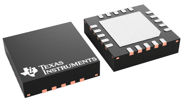
TPA6130A2 packaging includes a 2 by 2 mm chip-scale package, and a 4 by 4 mm QFN package.


