| Sample rate (Max) (MSPS) | 170 |
| Resolution (Bits) | 14 |
| Number of input channels | 1 |
| Interface type | Parallel CMOS, Parallel LVDS |
| Analog input BW (MHz) | 500 |
| Features | High Performance |
| Rating | Catalog |
| Input range (Vp-p) | 2 |
| Power consumption (Typ) (mW) | 1100 |
| Architecture | Pipeline |
| SNR (dB) | 74.3 |
| ENOB (Bits) | 12 |
| SFDR (dB) | 90 |
| Operating temperature range (C) | -40 to 85 |
| Input buffer | No |
- Maximum Sample Rate: 170 MSPS
- 14-Bit Resolution
- No Missing Codes
- Total Power Dissipation 1.1 W
- Internal Sample and Hold
- 74-dBFS SNR at 70-MHz IF
- 85-dBc SFDR at 70-MHz IF, 0 dB gain
- 11.4 ENOB Minimum at 70-MHz IF
- Double Data Rate (DDR) LVDS and Parallel CMOS Output Options
- Programmable Gain up to 6 dB for SNR/SFDR Trade-Off at High IF
- Reduced Power Modes at Lower Sample Rates
- Supports input clock amplitude down to 400 mVPP
- Clock Duty Cycle Stabilizer
- No External Reference Decoupling Required
- Internal and External Reference Support
- Programmable Output Clock position to ease data capture
- 3.3-V Analog and Digital Supply
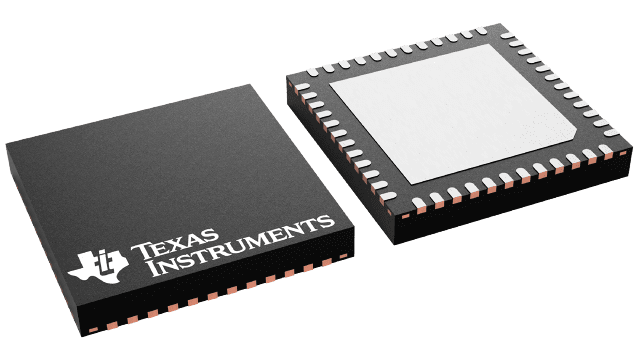
- 48-QFN Package (7 mm × 7 mm)
- APPLICATIONS
- Wireless Communications Infrastructure
- Software Defined Radio
- Power Amplifier Linearization
- 802.16d/e
- Test and Measurement Instrumentation
- High Definition Video
- Medical Imaging
- Radar Systems
ADS5545 is a high performance 14-bit, 170-MSPS A/D converter. It offers state-of-the-art functionality and performance using advanced techniques to minimize board space. Using an internal sample and hold and low jitter clock buffer, the ADC supports both high SNR and high SFDR at high input frequencies. It features programmable gain options that can be used to improve SFDR performance at lower full-scale analog input ranges.
In a compact 48-pin QFN, the device offers fully differential LVDS DDR (Double Data Rate) interface while parallel CMOS outputs can also be selected. Flexible output clock position programmability is available to ease capture and trade-off setup for hold times. At lower sampling rates, the ADC can be operated at scaled down power with no loss in performance. ADS5545 includes an internal reference, while eliminating the traditional reference pins and associated external decoupling. The device also supports an external reference mode.
The device is specified over the industrial temperature range (-40°C to 85°C).


