| Resolution (Bits) | 10 |
| Number of input channels | 4 |
| Sample rate (Max) (kSPS) | 400 |
| Interface type | SPI |
| Architecture | SAR |
| Input type | Pseudo-Differential, Single-Ended |
| Multi-channel configuration | Multiplexed |
| Rating | Catalog |
| Reference mode | Ext, Int |
| Input range (Max) (V) | 5.5 |
| Input range (Min) (V) | 0 |
| Operating temperature range (C) | -40 to 85 |
| Power consumption (Typ) (mW) | 10 |
| Analog voltage AVDD (Min) (V) | 4.5 |
| SNR (dB) | 60 |
| Analog voltage AVDD (Max) (V) | 5.5 |
| INL (Max) (+/-LSB) | 0.5 |
| Digital supply (Min) (V) | 4.5 |
| Digital supply (Max) (V) | 5.5 |
- Maximum Throughput 400 KSPS
- Built-In Reference and 8× FIFO
- Differential/Integral Nonlinearity Error:
±0.5 LSB Max - Signal-to-Noise and Distortion Ratio:
59 dB, fi = 12 kHz - Spurious Free Dynamic Range: 72 dB,
fi = 12 kHz - SPI/DSP-Compatible Serial Interfaces With SCLK up to 20 MHz
- Single Supply 5 Vdc
- Analog Input Range 0 V to Supply Voltage With 500 kHz BW
- Hardware Controlled and Programmable Sampling Period
- Low Operating Current (4 mA at 5.5 V External Ref, 6 mA at 5.5 V, Internal Ref)
- Power Down: Software/Hardware Power-Down Mode (1 uA Max, Ext Ref),
Auto Power-Down Mode (5 uA, Ext Ref) - Programmable Auto-Channel Sweep
- Pin Compatible, 12-Bit Upgrades Available
(TLC2554, TLC2558)
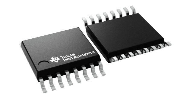
The TLC1518 and TLC1514 are a family of high-performance, 10-bit, low power, 1.4 us, CMOS SAR analog-to-digital converters (ADC) which operate from a single 5 V power supply. These devices have three digital inputs and a 3-state output [chip select (CS\), serial input-output clock (SCLK), serial data input (SDI), and serial data output (SDO)] that provide a direct 4-wire interface to the serial port of most popular host microprocessors (SPI interface). When interfaced with a DSP, a frame sync (FS) signal is used to indicate the start of a serial data frame.
In addition to a high-speed A/D converter and versatile control capability, these devices have an on-chip analog multiplexer that can select any analog inputs or one of three internal self-test voltages. The sample-and-hold function is automatically started after the fourth SCLK edge (normal sampling) or can be controlled by a special pin, CSTART\, to extend the sampling period (extended sampling). The normal sampling period can also be programmed as short (12 SCLKs) or as long (24 SCLKs) to accommodate faster SCLK operation popular among high-performance signal processors. The TLC1518 and TLC1514 are designed to operate with very low power consumption. The power-saving feature is further enhanced with software/hardware/auto power down modes and programmable conversion speeds. The converter uses the external SCLK as the source of the conversion clock. There is a 4-V internal reference available and an optional external reference can also be used to achieve maximum flexibility.
Free Data Converter Software Drivers for Code Composer Studio?
The data converter software drivers for TI's Code Composer Studio are just one of the benefits developers can realize from the eXpressDSP? Open Plug-in Architecture. The data converter software drivers provide software support for TI's data converters and TI's TMS320C5000? and TMS320C6000? DSP platforms. To download the software drivers, please visit our Web site at www.ti.com/sc/dcplug-in


