| Technology Family | CD4000 |
| Supply voltage (Min) (V) | 3 |
| Supply voltage (Max) (V) | 18 |
| Number of channels (#) | 4 |
| IOL (Max) (mA) | 11.2 |
| ICC (Max) (uA) | 3000 |
| IOH (Max) (mA) | -4.8 |
| Input type | Standard CMOS |
| Output type | Push-Pull |
| Features | Standard speed (tpd > 50ns), Input clamp diode |
| Rating | Catalog |
- Operation of liquid crystals with CMOS circuits provides ultra-low-power displays
- Equivalent ac output drive for liquid-crystal displays - no external capacitor required
- Voltage doubling across display, e.g. VDD - VEE = 18 V results in effective 36 V p-p drive across selected display segments
- Low- or high-output level dc drive for other types of displays
- On-chip logic-level conversion for different input- and output-level swings
- Full decoding of all input combinations: 0-9, L, H, P, A, -, and blank positions
- Strobed-latch function-CD4054B Series and CD4056B Series
- DISPLAY-FREQUENCY (DF) output for liquid-crystal common-line drive signal- CD4055B Series (CD4054B Series also: see introductory text)
- 100% tested for quiescent current at 20 V
- Maximum input current of 1 μA at 18 V over full package-temperature range; 100nA at 18 V and 25°C
- Noise margin (over full package-temperature range):
- 1 V at VDD = 5 V
- 2 V at VDD = 10 V
- 2.5 V at VDD = 15 V
- 5-V, 10-V, and 15-V parametric ratings
- Applications:
- General-purpose displays
- Calculators and meter
- Wall and table clocks
- Industrial control panels
- Portable lab instruments
- Panel meters
- Auto dashboard displays
- Appliance control panels
CD4055B and CD4056B types are single-digit BCD-to-7-segment decoder/driver circuits that provide level-shifting functions on the chip. This feature permits the BCD input-signal swings (VDD to VSS) to be the same as or different from the 7-segment output-signal swings (VDD to VEE). For example, the BCD input-signal (VDD to VSS) may be as small as 0 to -3 V, whereas the output-display drive-signal swing (VDD to VEE) may be as large as from 0 to -15 V. If VDD to VEE exceeds 15 V, VDD to VSS should be at least 4V (0 to -4V). The 7-segment outputs are controlled by the DISPLAY-FREQUENCY (DF) input which causes the selected segment outputs to be low, high, or a square-wave output (for liquid-crystal displays). When the DF input is low the output segments will be high when selected by the BCD inputs. When the DF input is high, the output segments will be low when selected by the BCD inputs. When a square-wave is present at the DF input, the selected segments will have a square-wave output that is 180° out of phase with the DF input. Those segments which are not selected will have a square-wave output that is in phase with the input. DF square-wave repetition rates for liquid-crystal displays usually range form 30 Hz (well above flicker rate) to 200 Hz (well below the upper limit of the liquid-crystal frequency response). The CD4055B provides a level-shifted high-amplitude DF output which is required for driving the common electrode in liquid-crystal displays. The CD4056B provides a strobed-latch function at the BCD inputs. Decoding of all input combinations on the CD4055B and CD4056B provides displays of 0 to 9 as well as L, P, H, A, -, and a blank position.
The CD4054B provides level shifting similar to the CD4055B and CD4056B independently strobed latches, and common DF control on 4 signal lines. The CD4054B is intended to provide drive-signal compatibility with the CD4055B and CD4056B 7-segment decoder types for the decimal point, colon, polarity, and similar display lines. A level-shifted high-amplitude DF output can be obtained from any CD4054B output line by connecting the corresponding input and strobe lines to a low and high level, respectively and applying a square wave to DFIN. The CD4054B may also be utilized for logic-level "up conversion" or "down conversion". For example, input-signal swings (VDD to VSS) for +5 to 0 V can be converted to output-signal swings (VDD to VEE) of +5 to -5 V. The level-shifted function on all three types permits the use of different input- and output-signal swings. The input swings from a low level of VSS to a high level of VDD while the output swings from a low level of VEE to the same high level of VDD. Thus, the input and output swings can be selected independently of each other over a 3-to 18 V range. VSS may be connected to VEE when no level-shift function is required.
For the CD4054B and CD4056B, data are transferred from input to output by placing a high voltage level at the strobe input. A low voltage at the strobe input latches the data input and the corresponding output segments remain selected (or non-selected) while the strobe is low.
Whenever the level-shifing function is required, the CD4055B can be used by itself to drive a liquid-crystal display (Fig.16 and Fig.20). The CD4056B, however, must be used together with a CD4054B to provide the common DF output (Fig.19). The capability of extending the voltage swing on the negative end (this voltage cannot be extended on the positive end) can be used to advantage in the setup of Fig.18. Fig.17 is common to all three types.
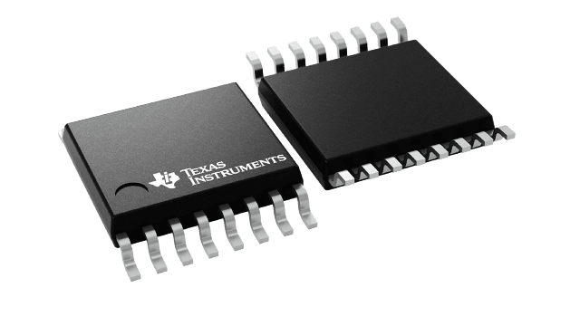
The CD4054B-, CD4055B-, and CD4056B-series types are supplied in 16-lead dual-in-line plastic packages (E suffix), 16-lead small-outline packages (M, M96, MT and NSR suffixes), and 16-lead thin shrink small-outline packages (PW and PWR suffixes). The CD4054B- and CD4056B-series types also are supplied in 16-lead hermetic dual-in-line ceramic packages (F3A suffix).


