| IOL (Max) (mA) | 64 |
| IOH (Max) (mA) | -32 |
| Technology Family | ABT |
| Rating | Catalog |
| Operating temperature range (C) | -40 to 85 |
| | |
- Members of the Texas Instruments SCOPETM Family of Testability Products
- Members of the Texas Instruments WidebusTM Family
- Compatible With the IEEE Standard 1149.1-1990 (JTAG) Test Access Port and Boundary-Scan Architecture
- Include D-Type Flip-Flops and Control Circuitry to Provide Multiplexed Transmission of Stored and Real-Time Data
- Bus Hold on Data Inputs Eliminates the Need for External Pullup Resistors
- B-Port Outputs of 'ABTH182646A Devices Have Equivalent 25-
 Series Resistors, So No External Resistors Are Required
 - State-of-the-Art EPIC-IIBTM BiCMOS Design
- One Boundary-Scan Cell Per I/O Architecture Improves Scan Efficiency
- SCOPETM Instruction Set
- IEEE Standard 1149.1-1990 Required Instructions and Optional CLAMP and HIGHZ
- Parallel-Signature Analysis at Inputs
- Pseudo-Random Pattern Generation From Outputs
- Sample Inputs/Toggle Outputs
- Binary Count From Outputs
- Device Identification
- Even-Parity Opcodes
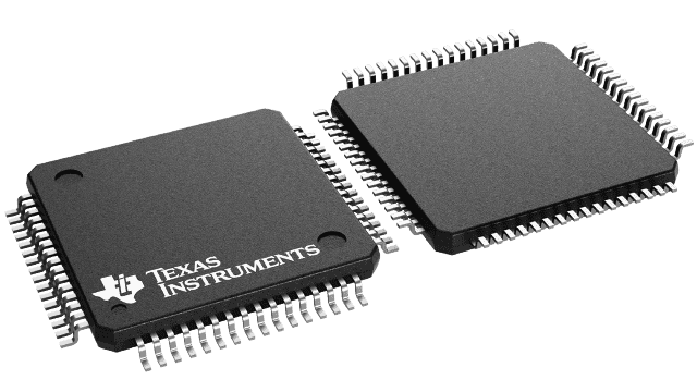
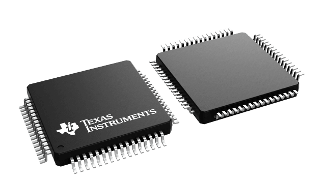
- Packaged in 64-Pin Plastic Thin Quad Flat (PM) Packages Using 0.5-mm Center-to-Center Spacings and 68-Pin Ceramic Quad Flat (HV) Packages Using 25-mil Center-to-Center Spacings
SCOPE, Widebus, and EPIC-IIB are trademarks of Texas Instruments Incorporated.
?
?
The 'ABTH18646A and 'ABTH182646A scan test devices with 18-bit bus transceivers and registers are members of the Texas Instruments SCOPETM testability integrated-circuit family. This family of devices supports IEEE Standard 1149.1-1990 boundary scan to facilitate testing of complex circuit-board assemblies. Scan access to the test circuitry is accomplished via the 4-wire test access port (TAP) interface.
In the normal mode, these devices are 18-bit bus transceivers and registers that allow for multiplexed transmission of data directly from the input bus or from the internal registers. They can be used either as two 9-bit transceivers or one 18-bit transceiver. The test circuitry can be activated by the TAP to take snapshot samples of the data appearing at the device pins or to perform a self test on the boundary-test cells. Activating the TAP in the normal mode does not affect the functional operation of the SCOPETM bus transceivers and registers.
Transceiver function is controlled by output-enable (![]() ) and direction (DIR) inputs. When
) and direction (DIR) inputs. When ![]() is low, the transceiver is active and operates in the A-to-B direction when DIR is high or in the B-to-A direction when DIR is low. When
is low, the transceiver is active and operates in the A-to-B direction when DIR is high or in the B-to-A direction when DIR is low. When ![]() is high, both the A and B outputs are in the high-impedance state, effectively isolating both buses.
is high, both the A and B outputs are in the high-impedance state, effectively isolating both buses.
Data flow is controlled by clock (CLKAB and CLKBA) and select (SAB and SBA) inputs. Data on the A bus is clocked into the associated registers on the low-to-high transition of CLKAB. When SAB is low, real-time A data is selected for presentation to the B bus (transparent mode). When SAB is high, stored A data is selected for presentation to the B bus (registered mode). The function of the CLKBA and SBA inputs mirrors that of CLKAB and SAB, respectively. Figure 1 shows the four fundamental bus-management functions that are performed with the 'ABTH18646A and 'ABTH182646A.
?
In the test mode, the normal operation of the SCOPETM bus transceivers and registers is inhibited, and the test circuitry is enabled to observe and control the I/O boundary of the device. When enabled, the test circuitry performs boundary-scan test operations according to the protocol described in IEEE Standard 1149.1-1990.
Four dedicated test pins observe and control the operation of the test circuitry: test data input (TDI), test data output (TDO), test mode select (TMS), and test clock (TCK). Additionally, the test circuitry performs other testing functions such as parallel-signature analysis (PSA) on data inputs and pseudo-random pattern generation (PRPG) from data outputs. All testing and scan operations are synchronized to the TAP interface.
Improved scan efficiency is accomplished through the adoption of a one boundary-scan cell (BSC) per I/O pin architecture. This architecture is implemented in such a way as to capture the most pertinent test data. A PSA/COUNT instruction also is included to ease the testing of memories and other circuits where a binary count addressing scheme is useful.
Active bus-hold circuitry holds unused or floating data inputs at a valid logic level.
The B-port outputs of 'ABTH182646A, which are designed to source or sink up to 12 mA, include 25-![]() series resistors to reduce overshoot and undershoot.
series resistors to reduce overshoot and undershoot.
The SN54ABTH18646A and SN54ABTH182646A are characterized for operation over the full military temperature range of -55°C to 125°C. The SN74ABTH18646A and SN74ABTH182646A are characterized for operation from -40°C to 85°C.
?
?
The data-output functions can be enabled or disabled by various signals at ![]() and DIR. Data-input functions are always enabled; i.e., data at the bus pins is stored on every low-to-high transition of the clock inputs.
and DIR. Data-input functions are always enabled; i.e., data at the bus pins is stored on every low-to-high transition of the clock inputs.


