| DSP | 1 C67x |
| DSP MHz (Max) | 200 |
| CPU | 32-/64-bit |
| Operating system | DSP/BIOS |
| Rating | Catalog |
| Operating temperature range (C) | 0 to 90 |
- C672x: 32-/64-Bit 350-MHz Floating-Point DSPs
- Upgrades to C67x+ CPU From C67x? DSP Generation:
- 2X CPU Registers [64 General-Purpose]
- New Audio-Specific Instructions
- Compatible With the C67x CPU
- Enhanced Memory System
- 256K-Byte Unified Program/Data RAM
- 384K-Byte Unified Program/Data ROM
- Single-Cycle Data Access From CPU
- Large Program Cache (32K Byte) Supports RAM, ROM, and External Memory
- External Memory Interface (EMIF) Supports
- 133-MHz SDRAM (16- or 32-Bit)
- Asynchronous NOR Flash, SRAM (8-,16-, or 32-Bit)
- NAND Flash (8- or 16-Bit)
- Enhanced I/O System
- High-Performance Crossbar Switch
- Dedicated McASP DMA Bus
- Deterministic I/O Performance
- dMAX (Dual Data Movement Accelerator) Supports:
- 16 Independent Channels
- Concurrent Processing of Two Transfer Requests
- 1-, 2-, and 3-Dimensional Memory-to-Memory and Memory-to-Peripheral Data Transfers
- Circular Addressing Where the Size of a Circular Buffer (FIFO) is not Limited to 2n
- Table-Based Multi-Tap Delay Read and Write Transfers From/To a Circular Buffer
- Three Multichannel Audio Serial Ports
- Transmit/Receive Clocks up to 50 MHz
- Six Clock Zones and 16 Serial Data Pins
- Supports TDM, I2S, and Similar Formats
- DIT-Capable (McASP2)
- Universal Host-Port Interface (UHPI)
- 32-Bit-Wide Data Bus for High Bandwidth
- Muxed and Non-Muxed Address and Data
- Two 10-MHz SPI Ports With 3-, 4-, and 5-Pin Options
- Two Inter-Integrated Circuit (I2C) Ports
- Real-Time Interrupt Counter/Watchdog
- Oscillator- and Software-Controlled PLL
- Applications:
- Professional Audio
- Mixers
- Effects Boxes
- Audio Synthesis
- Instrument/Amp Modeling
- Audio Conferencing
- Audio Broadcast
- Audio Encoder
- Emerging Audio Applications
- Biometrics
- Medical
- Industrial
- Professional Audio
- Commercial or Extended Temperature
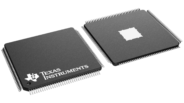
- 144-Pin, 0.5-mm, PowerPAD? Thin Quad Flatpack (TQFP) [RFP Suffix]
- 256-Terminal, 1.0-mm, 16x16 Array Plastic Ball Grid Array (PBGA) [GDH and ZDH Suffixes]
C67x, PowerPAD, TMS320C6000, C6000, DSP/BIOS, XDS, TMS320 are trademarks of Texas Instruments.
Philips is a registered trademark of Koninklijki Philips Electronics N.V.
All other trademarks are the property of their respective owners.
The TMS320C672x is the next generation of Texas Instruments' C67x generation of high-performance 32-/64-bit floating-point digital signal processors. The TMS320C672x includes the TMS320C6727B, TMS320C6726B, TMS320C6722B, and TMS320C6720 devices.(1)
Enhanced C67x+ CPU. The C67x+ CPU is an enhanced version of the C67x CPU used on the C671x DSPs. It is compatible with the C67x CPU but offers significant improvements in speed, code density, and floating-point performance per clock cycle. At 350 MHz, the CPU is capable of a maximum performance of 2800 MIPS/2100 MFLOPS by executing up to eight instructions (six of which are floating-point instructions) in parallel each cycle. The CPU natively supports 32-bit fixed-point, 32-bit single-precision floating-point, and 64-bit double-precision floating-point arithmetic.
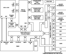
Efficient Memory System. The memory controller maps the large on-chip 256K-byte RAM and 384K-byte ROM as unified program/data memory. Development is simplified since there is no fixed division between program and data memory size as on some other devices.
The memory controller supports single-cycle data accesses from the C67x+ CPU to the RAM and ROM. Up to three parallel accesses to the internal RAM and ROM from three of the following four sources are supported:
- Two 64-bit data accesses from the C67x+ CPU
- One 256-bit program fetch from the core and program cache
- One 32-bit data access from the peripheral system (either dMAX or UHPI)
The large (32K-byte) program cache translates to a high hit rate for most applications. This prevents most program/data access conflicts to the on-chip memory. It also enables effective program execution from an off-chip memory such as an SDRAM.
High-Performance Crossbar Switch. A high-performance crossbar switch acts as a central hub between the different bus masters (CPU, dMAX, UHPI) and different targets (peripherals and memory). The crossbar is partially connected; some connections are not supported (for example, UHPI-to-peripheral connections).
Multiple transfers occur in parallel through the crossbar as long as there is no conflict between bus masters for a particular target. When a conflict does occur, the arbitration is a simple and deterministic fixed-priority scheme.
The dMAX is given highest-priority since it is responsible for the most time-critical I/O transfers, followed next by the UHPI, and finally by the CPU.
dMAX Dual Data Movement Accelerator. The dMAX is a module designed to perform Data Movement Acceleration. The Data Movement Accelerator (dMAX) controller handles user-programmed data transfers between the internal data memory controller and the device peripherals on the C672x DSPs. The dMAX allows movement of data to/from any addressable memory space including internal memory, peripherals, and external memory.
The dMAX controller includes features such as the capability to perform three-dimensional data transfers for advanced data sorting, and the capability to manage a section of the memory as a circular buffer/FIFO with delay-tap based reading and writing of data. The dMAX controller is capable of concurrently processing two transfer requests (provided that they are to/from different source/destinations).
External Memory Interface (EMIF) for Flexibility and Expansion. The external memory interface on the C672x supports a single bank of SDRAM and a single bank of asynchronous memory. The EMIF data width is 16 bits wide on the C6726B, C6722B, and C6720 and 32 bits wide on the C6727B.
SDRAM support includes x16 and x32 SDRAM devices with 1, 2, or 4 banks.
The C6726B, C6722B, and C6720 support SDRAM devices up to 128M bits.
The C6727B extends SDRAM support to 256M-bit and 512M-bit devices.
Asynchronous memory support is typically used to boot from a parallel non-multiplexed NOR flash device that can be 8, 16, or 32 bits wide. Booting from larger flash devices than are natively supported by the dedicated EMIF address lines is accomplished by using general-purpose I/O pins for upper address lines.
The asynchronous memory interface can also be configured to support 8- or 16-bit-wide NAND flash. It includes a hardware ECC calculation (for single-bit errors) that can operate on blocks of data up to 512 bytes.
Universal Host-Port Interface (UHPI) for High-Speed Parallel I/O. The Universal Host-Port Interface (UHPI) is a parallel interface through which an external host CPU can access memories on the DSP.
Three modes are supported by the C672x UHPI:
- Multiplexed Address/Data - Half-Word (16-bit-wide) Mode (similar to C6713)
- Multiplexed Address/Data - Full Word (32-bit-wide) Mode
- Non-Multiplexed Mode - 16-bit Address and 32-bit Data Bus
The UHPI can also be restricted to accessing a single page (64K bytes) of memory anywhere in the address space of the C672x; this page can be changed, but only by the C672x CPU. This feature allows the UHPI to be used for high-speed data transfers even in systems where security is an important requirement.
The UHPI is only available on the C6727B.
Multichannel Audio Serial Ports (McASP0, McASP1, and McASP2) - Up to 16 Stereo Channels I2S. The multichannel audio serial port (McASP) seamlessly interfaces to CODECs, DACs, ADCs, and other devices. It supports the ubiquitous IIS format as well as many variations of this format, including time division multiplex (TDM) formats with up to 32 time slots.
Each McASP includes a transmit and receive section which may operate independently or synchronously; furthermore, each section includes its own flexible clock generator and extensive error-checking logic.
As data passes through the McASP, it can be realigned so that the fixed-point representation used by the application code can be independent of the representation used by the external devices without requiring any CPU overhead to make the conversion.
The McASP is a configurable module and supports between 2 and 16 serial data pins. It also has the option of supporting a Digital Interface Transmitter (DIT) mode with a full 384 bits of channel status and user data memory.
McASP2 is not available on the C6722B and C6720.
Inter-Integrated Circuit Serial Ports (I2C0, I2C1). The C672x includes two inter-integrated circuit (I2C) serial ports. A typical application is to configure one I2C serial port as a slave to an external user-interface microcontroller. The other I2C serial port may then be used by the C672x DSP to control external peripheral devices, such as a CODEC or network controller, which are functionally peripherals of the DSP device.
The two I2C serial ports are pin-multiplexed with the SPI0 serial port.
Serial Peripheral Interface Ports (SPI0, SPI1). As in the case of the I2C serial ports, the C672x DSP also includes two serial peripheral interface (SPI) serial ports. This allows one SPI port to be configured as a slave to control the DSP while the other SPI serial port is used by the DSP to control external peripherals.
The SPI ports support a basic 3-pin mode as well as optional 4- and 5-pin modes. The optional pins include a slave chip-select pin and an enable pin which implements handshaking automatically in hardware for maximum SPI throughput.
The SPI0 port is pin-multiplexed with the two I2C serial ports (I2C0 and I2C1). The SPI1 serial port is pin-multiplexed with five of the serial data pins from McASP0 and McASP1.
Real-Time Interrupt Timer (RTI). The real-time interrupt timer module includes:
- Two 32-bit counter/prescaler pairs
- Two input captures (tied to McASP direct memory access [DMA] events for sample rate measurement)
- Four compares with automatic update capability
- Digital Watchdog (optional) for enhanced system robustness
Clock Generation (PLL and OSC). The C672x DSP includes an on-chip oscillator that supports crystals in the range of 12 MHz to 25 MHz. Alternatively, the clock can be provided externally through the CLKIN pin.
The DSP includes a flexible, software-programmable phase-locked loop (PLL) clock generator. Three different clock domains (SYSCLK1, SYSCLK2, and SYSCLK3) are generated by dividing down the PLL output. SYSCLK1 is the clock used by the CPU, memory controller, and memories. SYSCLK2 is used by the peripheral subsystem and dMAX. SYSCLK3 is used exclusively for the EMIF.
(1) Throughout the remainder of the document, TMS320C6727B (or C6727B), TMS320C6726B (or C6726B), TMS320C6722B (or C6722B), and/or TMS320C6720 (or C6720) will be referred to as TMS320C672x (or C672x).


