--- 產(chǎn)品詳情 ---
Bus voltage (Max) (V) | 110 |
Power switch | MOSFET |
Input VCC (Min) (V) | 8 |
Input VCC (Max) (V) | 17 |
Peak output current (A) | 3 |
Rise time (ns) | 8 |
Operating temperature range (C) | -40 to 140 |
Undervoltage lockout (Typ) | 8 |
Rating | Catalog |
Number of channels (#) | 2 |
Fall time (ns) | 7 |
Prop delay (ns) | 20 |
Iq (uA) | 1 |
Input threshold | TTL |
Channel input logic | TTL |
Negative voltage handling at HS pin (V) | -5 |
Driver configuration | Non-Inverting |
- Drives Two N-Channel MOSFETs in High-Side
and Low-Side Configuration - Negative Voltage Handling on HS (–5 V)
- Maximum Boot Voltage of 120 V
- Maximum VDD Voltage of 20 V
- On-Chip 0.65-V VF, 0.6-Ω RD Bootstrap Diode
- Greater than 1 MHz of Operation
- 20-ns Propagation Delay Times
- 3-A Sink and 3-A Source Output Currents
- 8-ns Rise and 7-ns Fall Time With 1000-pF Load
- 1-ns Delay Matching
- Undervoltage Lockout for High-Side and Low-Side
Driver - Specified from –40°C to 140°C
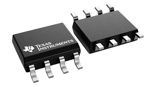
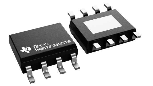
The UCC2720x family of high-frequency N-channel MOSFET drivers include a 120-V bootstrap diode and high-side and low-side drivers with independent inputs for maximum control flexibility. This allows for N-channel MOSFET control in half-bridge, full-bridge, two-switch forward, and active clamp forward converters. The low-side and the high-side gate drivers are independently controlled and matched to 1ns between the turnon and turnoff of each other.
An on-chip bootstrap diode eliminates the external discrete diodes. Undervoltage lockout is provided for both the high-side and the low-side drivers forcing the outputs low if the drive voltage is below the specified threshold.
Two versions of the UCC27200 are offered. The UCC27200 has high noise immune CMOS input thresholds while the UCC27201 has TTL compatible thresholds.
為你推薦
-
TI數(shù)字多路復(fù)用器和編碼器SN54HC1512022-12-23 15:12
-
TI數(shù)字多路復(fù)用器和編碼器SN54LS1532022-12-23 15:12
-
TI數(shù)字多路復(fù)用器和編碼器CD54HC1472022-12-23 15:12
-
TI數(shù)字多路復(fù)用器和編碼器CY74FCT2257T2022-12-23 15:12
-
TI數(shù)字多路復(fù)用器和編碼器SN74LVC257A2022-12-23 15:12
-
TI數(shù)字多路復(fù)用器和編碼器SN74LVC157A2022-12-23 15:12
-
TI數(shù)字多路復(fù)用器和編碼器SN74ALS258A2022-12-23 15:12
-
TI數(shù)字多路復(fù)用器和編碼器SN74ALS257A2022-12-23 15:12
-
TI數(shù)字多路復(fù)用器和編碼器SN74ALS157A2022-12-23 15:12
-
TI數(shù)字多路復(fù)用器和編碼器SN74AHCT1582022-12-23 15:12
-
【PCB設(shè)計必備】31條布線技巧2023-08-03 08:09
相信大家在做PCB設(shè)計時,都會發(fā)現(xiàn)布線這個環(huán)節(jié)必不可少,而且布線的合理性,也決定了PCB的美觀度和其生產(chǎn)成本的高低,同時還能體現(xiàn)出電路性能和散熱性能的好壞,以及是否可以讓器件的性能達(dá)到最優(yōu)等。在上篇內(nèi)容中,小編主要分享了PCB線寬線距的一些設(shè)計規(guī)則,那么本篇內(nèi)容,將針對PCB的布線方式,做個全面的總結(jié)給到大家,希望能夠?qū)︷B(yǎng)成良好的設(shè)計習(xí)慣有所幫助。1走線長度1365瀏覽量 -
電動汽車直流快充方案設(shè)計【含參考設(shè)計】2023-08-03 08:08
大功率直流充電系統(tǒng)架構(gòu)大功率直流充電設(shè)計標(biāo)準(zhǔn)國家大功率充電標(biāo)準(zhǔn)“Chaoji”技術(shù)標(biāo)準(zhǔn)設(shè)計目標(biāo)是未來可實現(xiàn)電動汽車充電5分鐘行駛400公里。“Chaoji”技術(shù)標(biāo)準(zhǔn)主要設(shè)計參數(shù)如下:最大電壓:目前1000V(可擴(kuò)展到1500V);最大電流:帶冷卻系統(tǒng)500A(可擴(kuò)展到600A);不帶冷卻系統(tǒng)150-200A;最大功率:900KW。大功率直流充電系統(tǒng)架構(gòu)大功率 -
Buck電路的原理及器件選型指南2023-07-31 22:28
-
100W USB PD 3.0電源2023-07-31 22:27
-
千萬不要忽略PCB設(shè)計中線寬線距的重要性2023-07-31 22:27
想要做好PCB設(shè)計,除了整體的布線布局外,線寬線距的規(guī)則也非常重要,因為線寬線距決定著電路板的性能和穩(wěn)定性。所以本篇以RK3588為例,詳細(xì)為大家介紹一下PCB線寬線距的通用設(shè)計規(guī)則。要注意的是,布線之前須把軟件默認(rèn)設(shè)置選項設(shè)置好,并打開DRC檢測開關(guān)。布線建議打開5mil格點,等長時可根據(jù)情況設(shè)置1mil格點。PCB布線線寬01布線首先應(yīng)滿足工廠加工能力,1377瀏覽量 -
基于STM32的300W無刷直流電機(jī)驅(qū)動方案2023-07-06 10:02
如何驅(qū)動無刷電機(jī)?近些年,由于無刷直流電機(jī)大規(guī)模的研發(fā)和技術(shù)的逐漸成熟,已逐步成為工業(yè)用電機(jī)的發(fā)展主流。圍繞降低生產(chǎn)成本和提高運行效率,各大廠商也提供不同型號的電機(jī)以滿足不同驅(qū)動系統(tǒng)的需求。現(xiàn)階段已經(jīng)在紡織、冶金、印刷、自動化生產(chǎn)流水線、數(shù)控機(jī)床等工業(yè)生產(chǎn)方面應(yīng)用。無刷直流電機(jī)的優(yōu)點與局限性優(yōu)點:高輸出功率、小尺寸和重量、散熱性好、效率高、運行速度范圍寬、低 -
上新啦!開發(fā)板僅需9.9元!2023-06-21 17:43
-
參考設(shè)計 | 2KW AC/DC數(shù)字電源方案2023-06-21 17:43
-
千萬不能小瞧的PCB半孔板2023-06-21 17:34