| Number of channels (#) | 2 |
| Vin (Min) (V) | 3 |
| Vin (Max) (V) | 6 |
| Vout (Min) (V) | 2.5 |
| Vout (Max) (V) | 27 |
| Type | Inductive |
| Switching frequency (Max) (kHz) | 1200 |
| LED current per channel (mA) | 23 |
| Peak efficiency (%) | 85 |
| Topology | Boost |
| Features | Synchronous Rectification |
| Operating temperature range (C) | -40 to 85 |
- 2.5-V to 6-V Input Voltage Range
- Two Outputs Each up to 27 V
- 0.7-A Integrated Switch
- Built-In Power Diode
- 1.2-MHz PWM for WLED Driver
- PFM for OLED Supply
- Individually Programmable Output
- Input to Output Isolation
- Short-Circuit Protection
- Built-In Soft Start
- Overvoltage Protection
- Up to 82% Efficiency
- Up to 30 kHz PWM Dimming Frequency
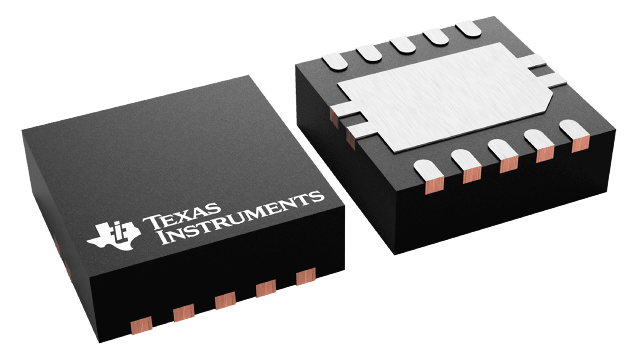
- Available in a 10 Pin, 3 × 3 mm QFN Package
- APPLICATIONS
- Clamshell Phone With OLED/LCD Screen
The TPS61140/1 is a dual output boost converter IC. It is intended to be configured as a highly integrated power solution providing regulated voltage and current output with one boost converter. This device is ideal for driving the OLED sub display and WLED backlight for the LCD main display in clam shell phones. The voltage and current can be individually programmed through external resistors. There is a dedicated selection pin for each output, so the two outputs can be turned on separately or simultaneously. When only the voltage output is enabled, the boost converter is controlled by pulse frequency modulation (PFM) in order to achieve high efficiency over a wide load range. If the current output is selected, the device adopts a 1.2-MHz pulse width modulation control (PWM) method in order to maximize output current. Applying an external PWM signal to the select pin (SELI) reduces the output current thereby allowing WLED dimming.
The TPS61140/1 has a built-in power MOSFET and power diode; thereby, eliminating the needs for any external active power components. In addition, the high switching frequency reduces the external inductor and capacitor sizes. Overall, the IC provides a highly compact solution with high efficiency and plenty of flexibility.


