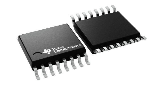
--- 產(chǎn)品詳情 ---
Number of channels (#) | 8 |
Topology | Current Sink, Open drain, Shift Register |
Rating | Automotive |
Operating temperature range (C) | -40 to 125 |
| |
Vin (Min) (V) | 4.5 |
Vin (Max) (V) | 5.5 |
Vout (Max) (V) | 33 |
Features | Enable/Shutdown, Thermal Shutdown |
- Low RDS(on), 7 &3937; (Typical)
- Avalanche Energy, 30 mJ
- Eight Power DMOS Transistor Outputs
of 100-mA Continuous Current - 250-mA Current Limit Capability
- ESD Protection, 2500 V
- Output Clamp Voltage, 33 V
- Enhanced Cascading for Multiple Stages
- All Registers Cleared With Single Input
- Low Power Consumption
The TPIC6C596 device is a monolithic, medium-voltage, low-current, 8-bit shift register designed for use in systems that require relatively moderate load power such as LEDs. The device contains a built-in voltage clamp on the outputs for inductive transient protection. Power driver applications include relays, solenoids, and other low-current or medium-voltage loads.
This device contains an 8-bit serial-in, parallel-out shift register that feeds an 8-bit D-type storage register. Data transfers through both the shift and storage registers on the rising edge of the shift register clock (SRCK) and the register clock (RCK), respectively. The storage register transfers data to the output buffer when shift register clear (CLR) is high. When CLR is low, all registers in the device are cleared. When output enable (G) is held high, all data in the output buffers is held low and all drain outputs are off. When G is held low, data from the storage register is transparent to the output buffers. When data in the output buffers is low, the DMOS transistor outputs are off. When data is high, the DMOS transistor outputs have sink-current capability.
The serial output (SER OUT) is clocked out of the device on the falling edge of SRCK to provide additional hold time for cascaded applications. This will provide improved performance for applications where clock signals may be skewed, devices are not located near one another, or the system must tolerate electromagnetic interference.
Outputs are low-side, open-drain DMOS transistors with output ratings of 33 V and 100 mA continuous sink-current capability. Each output provides a 250-mA maximum current limit at TC = 25°C. The current limit decreases as the junction temperature increases for additional device protection. The device also provides up to 2500 V of ESD protection when tested using the human body model and the 200-V machine model.
The TPIC6C596 device is characterized for operation over the operating case temperature range of ?40°C to 125°C.
為你推薦
-
TI數(shù)字多路復(fù)用器和編碼器SN54HC1512022-12-23 15:12
-
TI數(shù)字多路復(fù)用器和編碼器SN54LS1532022-12-23 15:12
-
TI數(shù)字多路復(fù)用器和編碼器CD54HC1472022-12-23 15:12
-
TI數(shù)字多路復(fù)用器和編碼器CY74FCT2257T2022-12-23 15:12
-
TI數(shù)字多路復(fù)用器和編碼器SN74LVC257A2022-12-23 15:12
-
TI數(shù)字多路復(fù)用器和編碼器SN74LVC157A2022-12-23 15:12
-
TI數(shù)字多路復(fù)用器和編碼器SN74ALS258A2022-12-23 15:12
-
TI數(shù)字多路復(fù)用器和編碼器SN74ALS257A2022-12-23 15:12
-
TI數(shù)字多路復(fù)用器和編碼器SN74ALS157A2022-12-23 15:12
-
TI數(shù)字多路復(fù)用器和編碼器SN74AHCT1582022-12-23 15:12
-
如何利用運(yùn)算放大器設(shè)計(jì)振蕩電路?2023-08-09 08:08
使用運(yùn)算放大器設(shè)計(jì)振蕩電路運(yùn)算放大器的工作原理發(fā)明運(yùn)算放大器的人絕對是天才。中間兩端接上電源,當(dāng)同相輸入大于反相輸入,右側(cè)就會輸出(接近)電源電壓(Vcc),如果反過來小于同相輸入,則輸出0V(負(fù)電源)電壓。在輸出端接上燈泡,假設(shè)我想控制燈泡循環(huán)亮滅,那就需要一會輸出高電平點(diǎn)亮,一會輸出低電平熄滅。也就是我需要讓左邊能自動變化大小,就能實(shí)現(xiàn)控制燈泡。如何讓電1609瀏覽量 -
【PCB設(shè)計(jì)必備】31條布線技巧2023-08-03 08:09
相信大家在做PCB設(shè)計(jì)時(shí),都會發(fā)現(xiàn)布線這個環(huán)節(jié)必不可少,而且布線的合理性,也決定了PCB的美觀度和其生產(chǎn)成本的高低,同時(shí)還能體現(xiàn)出電路性能和散熱性能的好壞,以及是否可以讓器件的性能達(dá)到最優(yōu)等。在上篇內(nèi)容中,小編主要分享了PCB線寬線距的一些設(shè)計(jì)規(guī)則,那么本篇內(nèi)容,將針對PCB的布線方式,做個全面的總結(jié)給到大家,希望能夠?qū)︷B(yǎng)成良好的設(shè)計(jì)習(xí)慣有所幫助。1走線長度1351瀏覽量 -
電動汽車直流快充方案設(shè)計(jì)【含參考設(shè)計(jì)】2023-08-03 08:08
大功率直流充電系統(tǒng)架構(gòu)大功率直流充電設(shè)計(jì)標(biāo)準(zhǔn)國家大功率充電標(biāo)準(zhǔn)“Chaoji”技術(shù)標(biāo)準(zhǔn)設(shè)計(jì)目標(biāo)是未來可實(shí)現(xiàn)電動汽車充電5分鐘行駛400公里。“Chaoji”技術(shù)標(biāo)準(zhǔn)主要設(shè)計(jì)參數(shù)如下:最大電壓:目前1000V(可擴(kuò)展到1500V);最大電流:帶冷卻系統(tǒng)500A(可擴(kuò)展到600A);不帶冷卻系統(tǒng)150-200A;最大功率:900KW。大功率直流充電系統(tǒng)架構(gòu)大功率 -
Buck電路的原理及器件選型指南2023-07-31 22:28
Buck電路工作原理電源閉合時(shí)電壓會快速增加,當(dāng)斷開時(shí)電壓會快速減小,如果開關(guān)速度足夠快的話,是不是就能把負(fù)載,控制在想要的電壓值以內(nèi)呢?假設(shè)12V降壓到5V,也就意味著,MOS管開關(guān)需要42%時(shí)間導(dǎo)通,58%時(shí)間斷開。當(dāng)42%時(shí)間MOS管導(dǎo)通時(shí),電感被充磁儲能,同時(shí)對電容進(jìn)行充電,給負(fù)載提供電量。當(dāng)58%時(shí)間MOS管斷開時(shí),由于電感上的電流不能突變,電路通 -
100W USB PD 3.0電源2023-07-31 22:27
-
千萬不要忽略PCB設(shè)計(jì)中線寬線距的重要性2023-07-31 22:27
想要做好PCB設(shè)計(jì),除了整體的布線布局外,線寬線距的規(guī)則也非常重要,因?yàn)榫€寬線距決定著電路板的性能和穩(wěn)定性。所以本篇以RK3588為例,詳細(xì)為大家介紹一下PCB線寬線距的通用設(shè)計(jì)規(guī)則。要注意的是,布線之前須把軟件默認(rèn)設(shè)置選項(xiàng)設(shè)置好,并打開DRC檢測開關(guān)。布線建議打開5mil格點(diǎn),等長時(shí)可根據(jù)情況設(shè)置1mil格點(diǎn)。PCB布線線寬01布線首先應(yīng)滿足工廠加工能力,1333瀏覽量 -
基于STM32的300W無刷直流電機(jī)驅(qū)動方案2023-07-06 10:02
如何驅(qū)動無刷電機(jī)?近些年,由于無刷直流電機(jī)大規(guī)模的研發(fā)和技術(shù)的逐漸成熟,已逐步成為工業(yè)用電機(jī)的發(fā)展主流。圍繞降低生產(chǎn)成本和提高運(yùn)行效率,各大廠商也提供不同型號的電機(jī)以滿足不同驅(qū)動系統(tǒng)的需求。現(xiàn)階段已經(jīng)在紡織、冶金、印刷、自動化生產(chǎn)流水線、數(shù)控機(jī)床等工業(yè)生產(chǎn)方面應(yīng)用。無刷直流電機(jī)的優(yōu)點(diǎn)與局限性優(yōu)點(diǎn):高輸出功率、小尺寸和重量、散熱性好、效率高、運(yùn)行速度范圍寬、低 -
上新啦!開發(fā)板僅需9.9元!2023-06-21 17:43
-
參考設(shè)計(jì) | 2KW AC/DC數(shù)字電源方案2023-06-21 17:43
-
千萬不能小瞧的PCB半孔板2023-06-21 17:34