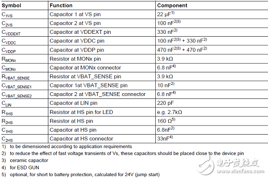
Infineon公司的TLE9842-2QX是TLE984x系列中一員,集成了32位ARM? Cortex? M0 MCU核,繼電器驅(qū)動(dòng)器,高邊開關(guān),LIN收發(fā)器和能工作在汽車電池的電源系統(tǒng).時(shí)鐘高達(dá)40MHz,具有單周期的乘法器,集成了40KB閃存,4KB EEPROM,768B 100次可編存儲(chǔ)器(100TP),2KB RAM以及引導(dǎo)ROM,工作電壓3.0 V到 28 V,工作溫度-40℃ 到150℃,主要用在汽車窗提升,汽車天窗,雨刷,泵馬達(dá)控制,風(fēng)扇馬達(dá)控制等.本文介紹了TLE9842-2QX主要特性,功能框圖,簡(jiǎn)化應(yīng)用框圖及所用外接元件表以及TLE984x系列評(píng)估板主要特性,框圖,電路圖,材料清單和PCB設(shè)計(jì)圖.
TLE9842-2QX is a part of the TLE984x product family. The TLE984x product family integrates an ARM? Cortex? M0 microcontroller core along with relay drivers, high side switches, LIN transceiver and a power supply system that enables the device to operate at the vehicle battery level. The TLE984x family offers scalability in terms of Flash memory sizes ranging from 36kB to 64kB with pin-compatible devices.
The TLE984x family was specifically designed to fit to a wide range of LIN-slave applications where a small package form factor and a minimum number of external components are essential. The TLE984x product family is offered in a leadless VQFN-48 package to save board space.
TLE9842-2QX主要特性:
? 32-bit ARM Cortex-M0 Core
– up to 40 MHz clock frequency
– one clock per machine cycle architecture
– single cycle multiplier
? On-chip memory
– 40 KB Flash (including EEPROM)
– 4 KB EEPROM (emulated in Flash)
– 768 bytes 100 Time Programmable Memory (100TP)
– 2 KB RAM
– Boot ROM for startup firmware and Flash routines
? On-chip OSC
? 2 Low-Side Switches incl. PWM functionality, can be used e.g. as relay driver
? 2 High-Side Switches with cyclic sense option and PWM functionality, e.g. for supplying LEDs or switch panels(min. 150 mA)
? 5 High Voltage Monitor Input pins for wake-up and with cyclic sense with analog measurement option
? 10 General-purpose I/O Ports (GPIO)
? 6 Analog input Ports
? 10-Bit A/D Converter with 6 analog inputs + VBAT_SENSE + VS + 5 high voltage monitoring inputs
? 8-Bit A/D Converter with 7 inputs for voltage and temperature supervision
? Measurement unit with 12 channels together with the onboard 10-Bit A/D converter and data post processing
? 16-Bit timers - GPT12, Timer 2 and Timer 21
? Capture/compare unit for PWM signal generation (CCU6)
? 2 full duplex serial interfaces (UART1, UART2), UART1 with LIN support
? 2 synchronous serial channels (SSC1, SSC2)
? On-chip debug support via 2-wire SWD
? LIN Bootstrap loader to program the Flash via LIN (LIN BSL)
? 1 LIN 2.2 transceiver
? Single power supply from 3.0 V to 28 V
? Low-dropout voltage regulators (LDO)
? 5 V voltage supply VDDEXT for external loads (e.g. Hall-sensor)
? Core logic supply at 1.5 V
? Programmable window watchdog (WDT1) with independent on-chip clock source
? Power saving modes:
– Micro Controller Unit slow-down mode
– Sleep Mode with cyclic sense option
– Cyclic wake-up during Sleep Mode
– Stop Mode with cyclic sense option
? Power-on and undervoltage/brownout reset generator
? Overtemperature protection
? Short circuit protection for all voltage regulators and actuators (High Side, Low Side)
? Loss of clock detection with fail safe mode for power switches
? Temperature Range TJ: -40℃ up to 150℃
? Package VQFN-48-31 with LTI feature
? Green package (RoHS compliant)
? AEC Qualified
TLE9842-2QX目標(biāo)應(yīng)用:
Window Lift
Sunroof
Wiper
Fan/Blower Motor Control
Pump Motor Control.
LIN addressed Relay Motor Applications
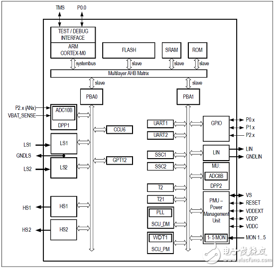
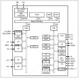
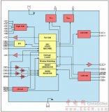
圖1.TLE9842-2QX框圖

圖2.TLE9842-2QX簡(jiǎn)化應(yīng)用框圖
圖2應(yīng)用框圖的外接元件表:
TLE984x系列評(píng)估板
The TLE984x Evaluation Board offers complete evaluation of all functions and peripherals of the TLE984x product family.This board is designed to provide a fast and easy start of evaluation, for Infineons embedded Power TLE984xdevice family. Initialy, the evaluation board brings several interfaces and interconnections.
The TLE984x device is placed in the center of the PCB. A socket provides the possibility to test and evaluate all ICsout of the TLE984x device family. Every pin of the IC is connectable via rows of pinheader. The board is protectedagainst reverse polarity of input voltage supply. A bidirectional relay can be connected to the integrated lowsideswitches, optionaly. In addition to that, a scew-connector is placed near the relay to contact and drive a DCmotor(example: window lift motor).
The evaluationboard provides an on board debugger. It provides a SWDDebugconnection and a virtual COM port for serial UART communication.Highside and Lowside switches and VDDEXT are connectable via 4mm standard laboratory wires.
The High-Voltage-Monitor pins can be triggered with dedicated pushbuttons.For analog input values a potentiometer is connected to PIN P2.2.The LIN connection is able to be configured to master and slave mode.
TLE984x系列評(píng)估板目標(biāo)應(yīng)用:
Motor Control & Drives
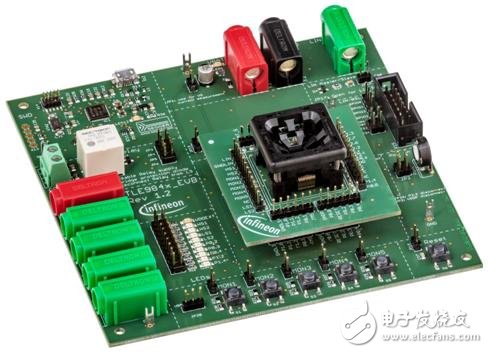
圖2.TLE984x系列評(píng)估板外形圖
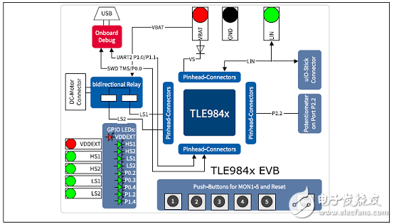
圖3.TLE984x系列評(píng)估板框圖
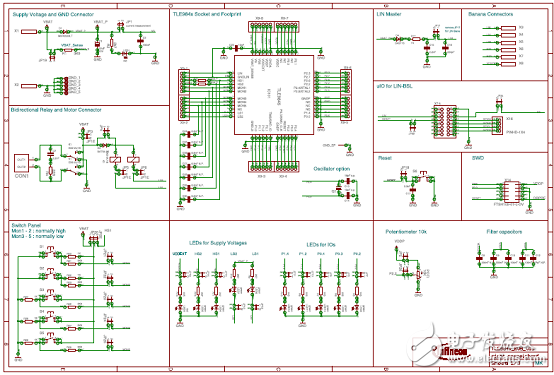
圖4.TLE984x系列評(píng)估板電路圖(1)

圖5.TLE984x系列評(píng)估板電路圖(2)
TLE984x系列評(píng)估板材料清單(BOM):
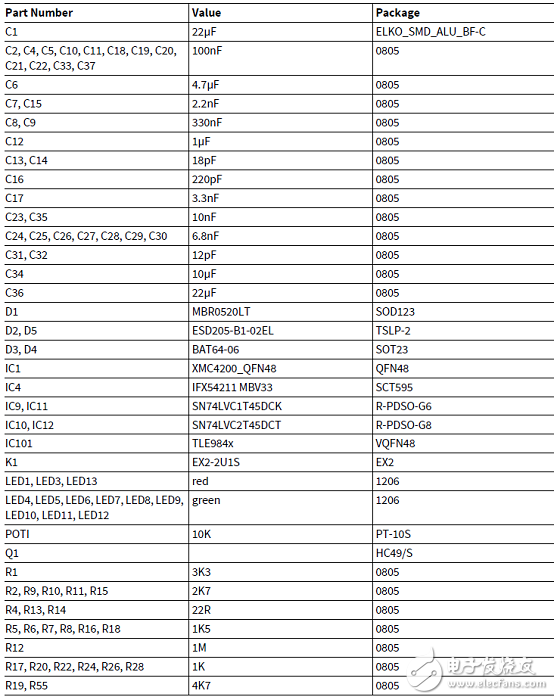
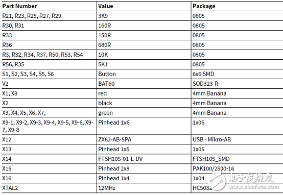
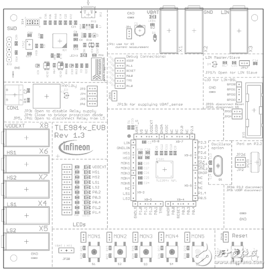
圖6.TLE984x系列評(píng)估板PCB元件布局圖
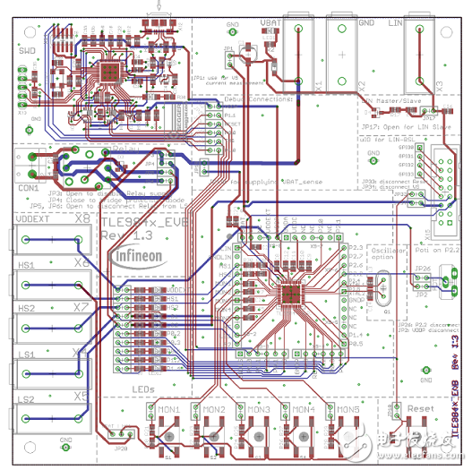
圖7.TLE984x系列評(píng)估板PCB設(shè)計(jì)合成圖
 電子發(fā)燒友App










評(píng)論