 電子發(fā)燒友App


要:本應(yīng)用筆記說明了如何計算DS31256 HDLC控制器的總線帶寬。并展示了一個實驗室實測的結(jié)果。同時演示了一個總線利用率速算表,該速算表如果需要可以索要。
根據(jù)本應(yīng)用筆記所提供的信息,用戶只需適當調(diào)整速算表(備索)中的一些數(shù)據(jù),就可將它用于特定的應(yīng)用中。
表1. 本應(yīng)用筆記所涉及到的變量的定義
表2. DMA讀所需的總線周期總數(shù)
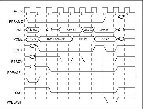
圖1. DS31256 PCI總線讀
表3. DMA寫所需的總線周期總數(shù)

圖2. DS31256 PCI總線寫周期
注意:對于訪問類型3和4,7個訪問周期是DS31256所固有的,不能改變。
Ct = [(3 + R + 12)/12] + [2 + R + 1] + [3 + R + 4] + [(P/4) + (3 + R)X] + [(2 + R + 6)/6] + [4(7/B)]
Cr = [(3 + R + 24)/12] + [(P/4) + (2 + R)X] + [2 + R + 3] + [(2 + R + 6)/6] + [4(7/B)]
表4. 為了便于計算每個包所需總線周期數(shù)所作的假設(shè)
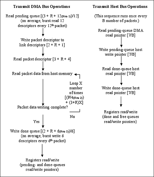
圖3. 每個包的總線處理流程
注:
圖3. (續(xù))
注:
公式1:

公式2:

注:

表5. PCI總線利用率實驗室實測數(shù)據(jù)
* 注:
注:
其中,1024 blocks是FIFO的尺寸,F(xiàn)IFO的高、低水印被設(shè)置于50%。
概述
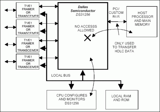
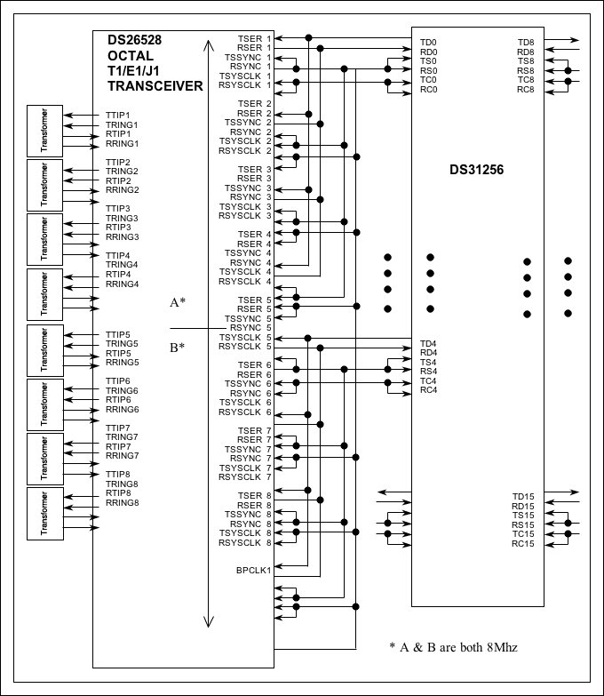
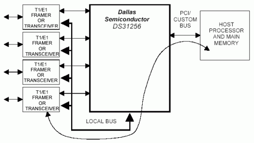
DS31256 HDLC控制器通過PCI總線存取發(fā)送和收到的HDLC包。本應(yīng)用筆記討論如何計算DS31256正常工作所需的總線帶寬。所涉及到的相關(guān)術(shù)語的定義在本文的開始部分給出。根據(jù)本應(yīng)用筆記所提供的信息,用戶只需適當調(diào)整速算表(備索)中的一些數(shù)據(jù),就可將它用于特定的應(yīng)用中。
表1. 本應(yīng)用筆記所涉及到的變量的定義
| Variable | Definition | Valid Range |
| B | Average number of packets processed before the host updates the receive free queue and transmit pending queue or reads the receive done queue and transmit done queue | 1, 2, 3, . . . . |
| C | Average number of bus cycles required per packet | 1, 2, 3, . . . . |
| D | Number of bus cycles needed for data to be transferred | 1, 2, 3, . . . . |
| P | Packet size in bytes | 64 |
| R | Average number of bus cycles added due to latency in RAM access | 0, 1, 2, . . . . |
| X | Average number of bus accesses required to send or obtain packet data to, or from the data buffers | 1, 2, 3, . . . . |
總線訪問類型
DS31256或主機執(zhí)行四種類型的總線訪問,以支持DS31256內(nèi)的直接存儲器訪問(DMA)。在下面的討論中,變量D定義為數(shù)據(jù)周期數(shù),變量R定義為由于RAM訪問時間的關(guān)系,所需要的總線周期數(shù)。訪問類型1:DMA突發(fā)讀主機RAM
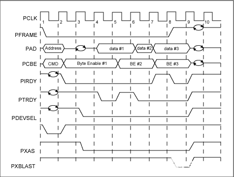
當DMA突發(fā)讀主機RAM時所需要的總線周期總數(shù)為[3+R+D]。這可由圖1和表2得出。表2. DMA讀所需的總線周期總數(shù)
| Cycle | No. Cycles Required |
| Address Cycle | 1 |
| Turnaround Cycle | 1 |
| RAM Access Latency Cycle | R |
| Data Cycle | D |
| Turnaround Cycle | 1 |
圖1. DS31256 PCI總線讀
訪問類型2:DMA突發(fā)寫主機RAM
當DMA突發(fā)寫主機RAM時所需的總線周期總數(shù)為[2+R+D]。這可從圖2和表3得到。表3. DMA寫所需的總線周期總數(shù)
| Cycle | No. Cycles Required |
| Address Cycle | 1 |
| RAM Access Latency Cycle | R |
| Data Cycle | D |
| Turnaround Cycle | 1 |
圖2. DS31256 PCI總線寫周期
訪問類型3:主機寫DS31256
主機寫入DS31256時所需的總線周期總數(shù)為7。訪問類型4:主機讀DS31256
主機讀取DS31256時所需的總線周期總數(shù)為7。注意:對于訪問類型3和4,7個訪問周期是DS31256所固有的,不能改變。
每個包所需的總線周期數(shù)
為計算總線利用率,首先必須知道所需要的總線周期數(shù)。為得到該數(shù)據(jù),我們做了一些假設(shè)列于表4。圖3給出了在收到或發(fā)出一個數(shù)據(jù)包時主機和DMA將要執(zhí)行的標準流程。根據(jù)圖3,我們有可能得出一個公式,來計算每個包所需要的平均總線周期數(shù),即變量C。發(fā)送側(cè)
發(fā)送側(cè)周期 = 讀等待隊列 + 寫水平描述符鏈 + 讀描述符 + 從主機存儲器讀取包 + 寫完成隊列 + 讀/寫寄存器。Ct = [(3 + R + 12)/12] + [2 + R + 1] + [3 + R + 4] + [(P/4) + (3 + R)X] + [(2 + R + 6)/6] + [4(7/B)]
接收側(cè)
接收側(cè)周期 = 讀自由隊列 + 將包寫入主機存儲器 + 寫描述符 + 寫完成隊列 + 讀/寫寄存器。Cr = [(3 + R + 24)/12] + [(P/4) + (2 + R)X] + [2 + R + 3] + [(2 + R + 6)/6] + [4(7/B)]
總公式
Ct + Cr = 21.16 + 3.5R + 0.5P + (5 + 2R)X + 56/B表4. 為了便于計算每個包所需總線周期數(shù)所作的假設(shè)
| 1 | All packets are 64 bytes (seen as worst case). |
| 2 | The Frame Check Sequence (FCS) of the HDLC packet is not transferred to, or from the PCI bus. |
| 3 | On the receive side, only large buffers are used (small buffers are disabled). |
| 4 | The receive DMA will burst read the free queue and burst write the done queue. |
| 5 | The transmit DMA will burst read the pending queue and burst write the done queue. |
| 6 | All packets fit within a single buffer (i.e., only one descriptor). This is reasonable because packets are 64 bytes. |
| 7 | All physical layer links are filled with packets; no idle codes are sent or received. |
| 8 | Interrupt routines and overhead (like accesses to the local bus) are not considered. |
圖3. 每個包的總線處理流程
注:
- 12個描述符 x 1雙字 = 12個發(fā)送等待隊列描述符雙字
- 包數(shù)據(jù)字節(jié)數(shù) = 4字節(jié)/數(shù)據(jù)周期
- 6個描述符 x 1雙字 = 6個發(fā)送完成隊列描述符雙字
圖3. (續(xù))
注:
- 12個描述符 x 2雙字 = 24個接收自由隊列描述符雙字
- 包數(shù)據(jù)字節(jié)數(shù) = 4字節(jié)/數(shù)據(jù)周期
- 6個描述符 x 1雙字 = 6個接收完成隊列描述符雙字
PCI總線利用率
總線利用率定義為DS31256每秒所需的總線周期數(shù)除以每秒可供使用的總線周期總數(shù)。總線利用率可按照特定的HDLC配置和業(yè)務(wù)量計算。計算中假定PCI總線時鐘速率為33MHz (33,000,000Hz),并且只用一片DS31256。以下就是PCI總線利用率的詳細計算方法。公式1:
公式2:
注:
舉例
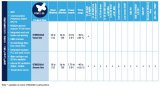
有關(guān)PCI總線利用率的實驗室測量結(jié)果展示了DS31256的PCI總線使用情況。其中假定所有收到的和發(fā)出的數(shù)據(jù)包都為56字節(jié)長(P = 56)。結(jié)果歸納于表5。我們還制作了一個可以計算總線利用率的速算表(如表6所示),如果需要可以索要(請聯(lián)絡(luò) telecom.support@maxim-ic.com (English only)。)表5. PCI總線利用率實驗室實測數(shù)據(jù)
| ? | ? | B | P | R | ? | ? | ? | ? | ? |
| Mode | No. of Ports | Avg. No. Done Queues Entries Processed | Pkt Size (Bytes) | Avg. RAM Access Latency Cycles | No. of HDLC Channels | Total No. of Channels | Channel Data Rate (kbps) | PCI Clock Rate (MHz) | PCI Bus Util.(%) |
| High Speed | 3 | 14.17 | 56 | 8.35 | 1 | 3 | 52 | 52 | 47.55 |
| Unchannelized | 3 | 35.53 | 56 | 8.50 | 1 | 3 | 29 | 29 | 49.06 |
| Low Speed | 16 | 100.46 | 56 | 10.60 | 1 | 16 | 12 | 12 | 55.27 |
| Unchannelized | 16 | 24.30 | 56 | 10.24 | 1 | 16 | 10 | 10 | 52.54 |
| T1 | 16 | 8.081 | 56 | 7.1375 | 12 | 192 | 128 * | 1.544 | 18.26 |
| E1 | 16 | 8.154 | 56 | 7.8645 | 16 | 256 | 128 | 2.048 | 28.07 |
| 2E1 | 16 | 10.894 | 56 | 8.003 | 16 | 256 | 256 | 4.096 | 55.82 |
| 4E1 | 16 | 381.207 | 56 | 8.3123 | 8 | 128 | 1024 | 8.192 | 50.97 |
* 注:
- 每個T1幀有193位 = [(24時隙 x 8位) + 1個同步位]
- 每個時隙的數(shù)據(jù)速率為64,000位/秒
- (64,000位/秒)/8位 = 8,000幀/秒
- 每125微妙到達一個T1幀 = 1/(8,000幀)/秒
- 數(shù)據(jù)速率為1,536,000位/秒 = 24信道 x (8位/信道/幀) x (8,000幀/秒)
- 線路總速率為1,544,000位/秒 = [(24信道 x (8位/信道)) + (1同步(位/幀))] x (8,000幀/秒)
| Input Variables | ? | ? |
| B | 14.17 | The average number of packets processed before the host updates the Receive Free Queue and Transmit Pending Queue, or reads the Receive/Transmit Done Queues. |
| P | 56 | The size of the packet in bytes. |
| R | 8.35 | The average number of bus cycles added due to latency in RAM access. |
| Number of HDLC channels per DS31256 | 3 | Use 1 per active port when operating in unchannelized mode. |
| Channel Data Rate (kbps) | 52,000.00 | Note that T1 speed == 1536kbps. |
| Channel Utilization Rate | 39.5% | There can be time between packets in real applications. |
| PCI Clock Rate (MHz) | 33 | ? |
| PCI Latency/Transaction | 10 | This is based on the average number of cycles required to perform each of the transactions associated with processing a packet. Our designers use 10 in their simulations, which is fairly conservative. |
| Number of DS31256's on Bus | 1 | ? |
| Intermediate Variables | ? | ? |
| C | 104.04 | The average number of bus cycles required per packet. |
| X | 1.00 | The average number of bus accesses required to send/obtain packet data to/from the data buffers. |
| Packets/second/channel | 45,871.43 | ? |
| Total PCI Latency | 1,376,142.86 | ? |
| No. of Bus cycles required/sec | 15,693,122 | ? |
| Half Duplex | ? | Full Duplex |
| Bus utilization | 47.6% | 95.11% |
| Bus Capacity (Mbps) | 264 | ? |
| Bus Throughput (Mbps) | 125.54 | 251.09 |
注:
其中,1024 blocks是FIFO的尺寸,F(xiàn)IFO的高、低水印被設(shè)置于50%。


 工商網(wǎng)監(jiān)
評論