摘要:DS26502的數據資料包含了在各類應用中使用DS26502所需的所有信息。數據資料是為使用軟件模式的用戶而寫的,提供了通過控制寄存器配置DS26502所需的信息,但并沒有包含在硬件模式下如何配置DS26502的內容。
本應用筆記著重討論在硬件模式下使用DS26502的方法,不再贅述數據資料中已涵蓋的,只與軟件模式相關的內容。
硬件模式是否可用取決于具體應用的特殊要求。設計者需要重點考慮的是,確定目標應用是否會用到一些只能在軟件模式下使用的功能。表1列出了所有只能在軟件模式下使用,硬件模式下不可用的功能。并給出了寄存器位及其名稱,以便于參照DS26502數據資料中的完整功能描述。
除了一些軟件可控的功能在硬件模式下完全喪失外,還有一些功能仍然存在,但不可更改。這些不可更改的功能如表3所示,是按照使用硬件模式的常規應用的要求精挑細選的。硬件模式下每個引腳功能的完整描述在表4中給出。圖1到圖4是DS26502硬件模式下的功能框圖。這些框圖與數據資料中所給出的軟件模式下的情況相似。不同的是,軟件模式中對應于控制寄存器的位置在這里被替換為DS26502的外部引腳。軟件模式特有的功能也被去掉了。
盡管大多數DS26502應用采用的是軟件模式,硬件模式對于許多用戶而言仍然是一個可用的選項。本應用筆記再加上DS26502數據資料所提供的信息,有助于設計者花費最少的時間和精力,構建并實施一個硬件模式的應用。
表1. 硬件模式中無法使用的軟件模式功能
表2. 硬件模式下的控制引腳與寄存器的對應關系
表3. 硬件模式默認功能
表4. 硬件模式下的引腳功能描述
發送側
接收側
控制器接口
發送通道工作模式
注1:DS26502內部沒有產生CAS信令和復幀同步碼的資源。必須將CAS信令和復幀同步碼嵌入到TSER引腳上的發送數據中(TS16時隙),幀與TS_8K_4引腳上的同步信號相對齊。
接收通道工作模式
E1線路補償
T1線路補償
注1:該模式下TTD引腳必須接高電平。
注2:N.M. = 無意義
JTAG
線路接口
電源
這些圖并未涉及所有DS26502的硬件模式引腳,只給出了那些需要在硬件模式下控制DS26502功能的引腳。本應用筆記的“引腳功能描述”部分給出了完整的引腳功能描述。以下引腳在框圖中沒有出現:RSM, TSM, TITD, RITD, E1TS, TAIS, L0, L1, L2, JACKS, HBE。
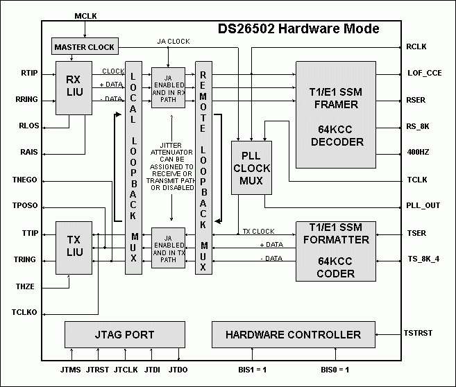
圖1. DS26502硬件模式框圖
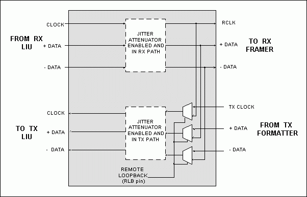
圖2. 環回復用器框圖
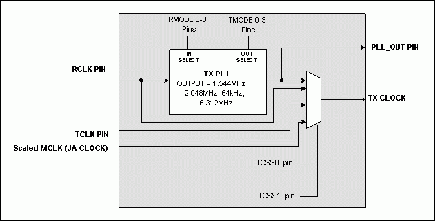
圖3. 發送PLL時鐘復用器框圖
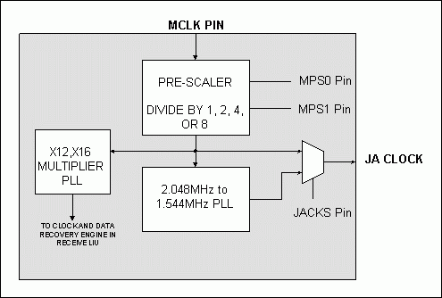
圖4. 主時鐘PLL框圖
本應用筆記著重討論在硬件模式下使用DS26502的方法,不再贅述數據資料中已涵蓋的,只與軟件模式相關的內容。
簡介
DS26502有兩種主要的操作模式:軟件模式和硬件模式。這里的“模式”是指器件的控制方式。采用軟件模式的應用利用微控制器的串行或并行總線與DS26502內部的控制寄存器通信,達到控制其工作的目的。在硬件模式中,串行/并行通信接口引腳被重新分配了新的功能,以便能夠通過這些引腳的邏輯狀態直接控制DS26502的內部工作。什么時候應該用硬件模式?
在硬件模式下使用DS26502的優點是無需用微控制器來控制其工作。硬件模式是否可用取決于具體應用的特殊要求。設計者需要重點考慮的是,確定目標應用是否會用到一些只能在軟件模式下使用的功能。表1列出了所有只能在軟件模式下使用,硬件模式下不可用的功能。并給出了寄存器位及其名稱,以便于參照DS26502數據資料中的完整功能描述。
硬件模式的實現
硬件模式下DS26502的工作受控于外部引腳。表2列出了軟件模式中的一些控制位和與之相對應的、用于在硬件模式下控制DS26502的引腳的作用。除了一些軟件可控的功能在硬件模式下完全喪失外,還有一些功能仍然存在,但不可更改。這些不可更改的功能如表3所示,是按照使用硬件模式的常規應用的要求精挑細選的。硬件模式下每個引腳功能的完整描述在表4中給出。圖1到圖4是DS26502硬件模式下的功能框圖。這些框圖與數據資料中所給出的軟件模式下的情況相似。不同的是,軟件模式中對應于控制寄存器的位置在這里被替換為DS26502的外部引腳。軟件模式特有的功能也被去掉了。
盡管大多數DS26502應用采用的是軟件模式,硬件模式對于許多用戶而言仍然是一個可用的選項。本應用筆記再加上DS26502數據資料所提供的信息,有助于設計者花費最少的時間和精力,構建并實施一個硬件模式的應用。
表1. 硬件模式中無法使用的軟件模式功能
| Register | Description |
| TSTRREG | Test Reset Register |
| IDR | Device Identification Register |
| INFO1 | Information Register 1 |
| INFO2 | Information Register 2 |
| IIR | Interrupt Information Register |
| SR1 | Status Register 1 |
| IMR1 | Interrupt Mask Register 1 |
| SR2.7 | Receive Yellow Alarm Clear Event |
| SR2.6 | Receive Alarm Indication Signal Clear Event |
| SR2.5 | Receive Loss Of Signal Clear Event |
| SR2.4 | Receive Loss of Frame Clear Event |
| SR2.3 | Receive Yellow Alarm Condition |
| IMR2 | Interrupt Mask Register 2 |
| SR3 | Status Register 3 |
| IMR3 | Interrupt Mask Register 3 |
| SR4 | Status Register 4 |
| IMR4 | Interrupt Mask Register 4 |
| INFO3 | Information Register 3 |
| RAF | Receive Align Frame Register |
| RNAF | Receive Non-Align Frame Register |
| RSiAF | Receive Si Bits of the Align Frame |
| RSiNAF | Receive Si Bits of the Non-Align Frame |
| RRA | Receive Remote Alarm |
| RSa4 | Receive Sa4 Bits |
| RSa5 | Receive Sa5 Bits |
| RSa6 | Receive Sa6 Bits |
| RSa7 | Receive Sa7 Bits |
| RSa8 | Receive Sa8 Bits |
| TEST1-16 | Test Register 1-16 |
表2. 硬件模式下的控制引腳與寄存器的對應關系
| Position | Pin | Name |
| IOCR1.5 | RSM | RS_8K Mode Select |
| IOCR1.2 | TSM | TS_8K_4 Mode Select |
| T1RCR2.5 | HBE | Receive B8ZS Enable |
| T1TCR2.7 | HBE | Transmit B8ZS Enable |
| MCREG.7 | TMODE3 | Transmit Mode Configuration 3 |
| MCREG.6 | TMODE2 | Transmit Mode Configuration 2 |
| MCREG.5 | TMODE1 | Transmit Mode Configuration 1 |
| MCREG.4 | TMODE0 | Transmit Mode Configuration 0 |
| MCREG.3 | RMODE3 | Receive Mode Configuration 3 |
| MCREG.2 | RMODE2 | Receive Mode Configuration 2 |
| MCREG.1 | RMODE1 | Receive Mode Configuration 1 |
| MCREG.0 | RMODE0 | Receive Mode Configuration 0 |
| TPCR.1 | TCSS1 | Transmit Clock (TX CLOCK) Source Select 1 |
| TPCR.0 | TCSS0 | Transmit Clock (TX CLOCK) Source Select 0 |
| SR2.2 | RAIS | Receive Alarm Indication Signal |
| SR2.1 | RLOS | Receive Loss Of Signal Condition |
| SR2.0 | RLOF_CCE | Receive Loss of Frame Condition |
| E1RCR.5 | HBE | Receive HDB3 Enable |
| E1TCR.1 | HBE | Transmit HDB3 Enable |
| LBCR.2 | RLB | Remote loopback enabled |
| LIC1.7 | L2 | Line Build-Out Select 2 |
| LIC1.6 | L1 | Line Build-Out Select 1 |
| LIC1.5 | L0 | Line Build-Out Select 0 |
| LIC2.4 | TAIS | Transmit Alarm Indication Signal |
| LIC2.3 | JACKS | Jitter Attenuator Mux |
| LIC4.7 | MPS1 | MCLK Prescaler 1 |
| LIC4.6 | MPS0 | MCLK Prescaler 0 |
表3. 硬件模式默認功能
| Position | Name | Hardware Mode Function |
| IOCR1.6 | RS_8K Mode Select 2 | T1 Mode: (when RMS = 0)do not pulse double-wide in signaling framesE1 Mode: (when RMS = 1)RS_8K outputs CAS multiframe boundaries |
| IOCR1.4 | RLOF_CCE Output Function | receive loss of frame (RLOF) |
| IOCR1.3 | Composite Clock Sync Mode_ Transmit Signaling Double-Wide Sync | (CC64K) 8kHz reference, (T1) normal sync pulses |
| IOCR1.1 | TS_8K_4 I/O Select | TS_8K_4 is an input |
| IOCR1.0 | Output Data Format | bipolar data at TPOS and TNEG |
| IOCR2.7 | RCLK | Invert no inversion |
| IOCR2.6 | TCLK | Invert no inversion |
| IOCR2.5 | RS_8K Invert | no inversion |
| IOCR2.4 | TS_8K_4 | Invert no inversion |
| T1RCR1.6 | Auto Resync Criteria | resync on OOF or RLOS event |
| T1RCR1.5T1RCR1.4 | Out Of Frame Select Bits | Out Of Frame Criteria2/4 frame bits in error |
| T1RCR1.3 | Sync Criteria | In D4 Framing Mode:search for Ft pattern, then search for Fs patternIn ESF Framing Mode:search for FPS pattern only |
| T1RCR1.2 | Sync Time | qualify 10 bits |
| T1RCR1.1 | Sync Enable | auto resync enabled |
| T1RCR1.0 | Resynchronize | No manual resynchronization of the receive side framer allowed |
| T1RCR2.1 | Receive Japanese CRC6 Enable | use ANSI/AT&T/ITU CRC6 calculation (normal operation)Japanese CRC6 not available |
| T1RCR2.0 | Receive Side D4 Yellow Alarm Select | zeros in bit 2 of all channels |
| T1TCR1.7 | Transmit Japanese CRC6 Enable | use ANSI/AT&T/ITU CRC6 calculation (normal operation)Japanese CRC6 not available |
| T1TCR1.6 | Transmit F-Bit Pass-Through | F bits sourced internally |
| T1TCR1.5 | Transmit CRC Pass-Through | source CRC6 bits internally |
| T1TCR1.0 | Transmit Yellow Alarm | cannot transmit yellow alarm |
| T1TCR2.6 | Transmit Fs-Bit Insertion Enable | Fs-bit insertion enabled |
| T1TCR2.4 | Bit 4/F-Bit Corruption Type 2 | No bit corruption support |
| T1TCR2.3 | F-Bit Corruption Type 1 | No bit corruption support |
| T1TCR2.2 | Transmit-Side D4 Yellow Alarm Select | 0s in bit 2 of all channels |
| T1TCR2.0 | Transmit-Side Bit 7 Zero-Suppression Enable | no stuffing occurs |
| T1CCR.4 | Transmit RAI-CI Enable | do not transmit the ESF RAI-CI code |
| T1CCR.3 | Transmit AIS-CI Enable | do not transmit the AIS-CI code |
| T1CCR.1 | Pulse-Density Enforcer Enable | disable transmit pulse-density enforcer |
| TPCR.7 | Transmit PLL Output Frequency Select 1 | in hardware mode, use TMODE pins |
| TPCR.6 | Transmit PLL Output Frequency Select 0 | in hardware mode, use TMODE pins |
| TPCR.5 | PLL_OUT Select | PLL_OUT is sourced directly from the TX PLL |
| TPCR.4 | Transmit PLL Input Frequency Select 0 | in hardware mode, use RMODE pins |
| TPCR.3 | Transmit PLL Input Frequency Select 1 | in hardware mode, use RMODE pins |
| TPCR.2 | Transmit PLL_CLK Source Select | Use the recovered network clock. This is the same clock available at the RCLK pin (output) |
| E1RCR.6 | Receive Loss Of Signal | RLOS declared upon 255 consecutive zeros (125μs) |
| E1RCR.2 | Frame Resync Criteria | resync if FAS received in error three consecutive times |
| E1RCR.1 | Sync Enable | auto resync enabled |
| E1RCR.0 | Resync | No manual resync |
| E1TCR.7 | Transmit Time Slot 0 Pass-Through | FAS bits/Sa bits/remote alarm sourced internally from the TAF and TNAF registers |
| E1TCR.4 | Transmit International Bit Select | sample Si bits at TSER pin |
| BOCC.4 | Receive BOC Enable | receive BOC function disabled |
| BOCC.3 | Receive BOC Reset | No manual reset of the BOC circuitry |
| BOCC.2 | Receive BOC Filter Bit 1 | sets the number of consecutive patterns that must be received without error prior to an indication of a valid message |
| BOCC.1 | Receive BOC Filter Bit 0 | sets the number of consecutive patterns that must be received without error prior to an indication of a valid message |
| BOCC.0 | Send BOC | Do not transmit BOC code |
| LBCR.3 | Local Loopback | Local loopback disabled |
| LIC1.4 | Receive Equalizer Gain Limit | T1 Mode: -36dB (long haul)E1 Mode: -43dB (long haul) |
| LIC1.3 | Jitter Attenuator Select | place the jitter attenuator on the receive side |
| LIC1.2 | Jitter Attenuator Buffer Depth Select | 128 bits |
| LIC1.1 | Disable Jitter Attenuator | jitter attenuator enabled |
| LIC1.0 | Transmit Power-Down normal | transmitter operation |
| LIC2.6 | Line Interface Reset | No manual reset supported |
| LIC2.5 | Insert BPV | No insert BPV supported |
| LIC2.2 | Receive Composite Clock Filter Enable | Receive Composite Clock Filter Disabled |
| LIC2.1 | Short Circuit Limit Disable (in E1 mode) | enable 50mA current limiter |
| LIC2.0 | Custom Line Driver Select | normal operation |
| LIC3.7 | CMI Enable | disable CMI mode |
| LIC3.6 | CMI Invert | CMI normal at TTIP and RTIP |
| LIC3.4 | Monitor Mode 1 | Normal operation (no boost) |
| LIC3.3 | Monitor Mode 0 | Normal operation (no boost) |
| LIC3.0 | Transmit Alternate Ones and Zeros | disabled |
| TLBC.6 | Automatic Gain Control Enable | use Transmit AGC, TLBC bits 0-5 are "don't care" |
| TLBC.5 | Gain Control Bit | Not used |
| TLBC.4 | Gain Control Bit | Not used |
| TLBC.3 | Gain Control Bit | Not used |
| TLBC.2 | Gain Control Bit | Not used |
| TLBC.1 | Gain Control Bit | Not used |
| TLBC.0 | Gain Control Bit | Not used |
| TAF.7 | International Bit | 0 |
| TAF.6 | Frame Alignment Signal Bit (0) | 0 |
| TAF.5 | Frame Alignment Signal Bit (0) | 0 |
| TAF.4 | Frame Alignment Signal Bit (1) | 1 |
| TAF.3 | Frame Alignment Signal Bit (1) | 1 |
| TAF.2 | Frame Alignment Signal Bit (0) | 0 |
| TAF.1 | Frame Alignment Signal Bit (1) | 1 |
| TAF.0 | Frame Alignment Signal Bit (1) | 1 |
| TNAF.7 | International Bit (Si) | 0 |
| TNAF.6 | Frame Nonalignment Signal Bit (1) | 1 |
| TNAF.5 | Remote Alarm (used to transmit the alarm A) | 0 |
| TNAF.4 | Additional Bit 4 (Sa4) | 0 |
| TNAF.3 | Additional Bit 5 (Sa5) | 0 |
| TNAF.2 | Additional Bit 6 (Sa6) | 0 |
| TNAF.1 | Additional Bit 7 (Sa7) | 0 |
| TNAF.0 | Additional Bit 8 (Sa8) | 0 |
| TSiAF.0-7 | Si Bit of Frames 0, 2, 4, 6, 8, 10, 12, 14 | 0 in all bit locations |
| TSiNAF.0-7 | Si Bit of Frames 1, 3, 5, 7, 9, 11, 13, 15 | 0 in all bit locations |
| TRA.0-7 | Remote Alarm Bit of Frame 1, 3, 5, 7, 9, 11, 13, 15 | 0 in all bit locations |
| TSa4.0-7 | Sa4 Bit of Frames 1, 3, 5, 7, 9, 11, 13, 15 | 0 in all bit locations |
| TSa5.0-7 | Sa5 Bit of Frames 1, 3, 5, 7, 9, 11, 13, 15 | 0 in all bit locations |
| TSa6.0-7 | Sa6 Bit of Frames 1, 3, 5, 7, 9, 11, 13, 15 | 0 in all bit locations |
| Tsa7.0-7 | Sa7 Bit of Frames 1, 3, 5, 7, 9, 11, 13, 15 | 0 in all bit locations |
| Tsa8.0-7 | Sa8 Bit of Frames 1, 3, 5, 7, 9, 11, 13, 15 | 0 in all bit locations |
| TSACR.0-7 | Insertion Control Bits for TsiAF, TSiNAF, TRA, TSa4, TSa5, TSa6, TSa7, TSa8 | do not insert data from the registers TsiAF, TSiNAF, TRA, TSa4, TSa5, TSa6, TSa7, TSa8 into the transmit data stream |
| RFDL.0-5 | BOC Bit 0-5 | 0 in all bit locations |
| TFDL.7 | Transmit FDL Bit 7 MSB of the transmit FDL code | 0 |
| TFDL.6 | Transmit FDL Bit 6 | 0 |
| TFDL.5 | Transmit FDL Bit 5 | 0 |
| TFDL.4 | Transmit FDL Bit 4 | 1 |
| TFDL.3 | Transmit FDL Bit 3 | 1 |
| TFDL.2 | Transmit FDL Bit 2 | 1 |
| TFDL.1 | Transmit FDL Bit 1 | 0 |
| TFDL.0 | Transmit FDL Bit 0 LSB of the transmit FDL code | 0 |
| RFDLM1.0-7 | Receive FDL Match Bit 0-7 | 0 in all bit locations |
| RFDLM2.0-7 | Receive FDL Match Bit 0-7 | 0 in all bit locations |
發送PLL
在硬件控制模式下,連接到發送PLL輸入的始終是TCLK引腳。發送時鐘由TCSS0和TCSS1引腳選擇。PLL_OUT引腳上的信號始終和選定的發送時鐘相同。如果用戶想使發送器工作于恢復出來的時鐘,可在外部將RCLK引腳連接到TCLK引腳。表4. 硬件模式下的引腳功能描述
| Pin | Name | Type | Function | |||||||||||||||
| 47 | PLL_OUT | O | Transmit PLL Output. 1544kHz, 2048kHz, 64kHz, or 6312kHz output from the internal TX PLL | |||||||||||||||
| 17 | TCLK | I | Transmit Clock Input. A 64kHz, 1.544MHz, 2.048MHz, or 6312kHz primary clock. By using TCSS0 and TCSS1 pins, may be selected by the TX PLL mux to provide a clock to the transmit section | |||||||||||||||
| 6331 | TCSS0 TCSS1 |
I | Transmit Clock Source Select 0 and 1 Selects the output of the TX PLL Clock Mux function.
|
發送側
| Pin | Name | Type | Function |
| 21 | TSER | I | Transmit Serial Data. Source of transmit data sampled on the falling edge of the selected transmit clock. In normal operation the selected transmit clock is output at the TCLKO pin. |
| 23 | TS_8K_4 | I | TSYNC, 8kHz Sync, 400Hz Sync (400Hz Sync N/A in HW mode.)T1/E1 Mode: A pulse at this pin will establish either frame or multiframe boundaries for the transmit side. 64KCC Mode: Establishes the boundary for the 8kHz portion of the composite clock. |
| 18 | TCLKO | O | Transmit Clock Output. In normal operation this output is the selected transmit clock from the TX_PLL, TCLK pin, or the recovered clock (RCLK). When remote loopback is enabled this pin will output the recovered network clock. |
| 20 | TPOSO | O | Transmit Positive-Data Output. In T1 or E1 mode, updated on the rising edge of TCLKO with the bipolar data out of the transmit-side formatter. In 64KCC or 6312 mode, this pin will be low. |
| 19 | TNEGO | O | Transmit Negative-Data Output. In T1 or E1 mode, updated on the rising edge of TCLKO with the bipolar data out of the transmit-side formatter. In 64KCC or 6312 mode, this pin will be low. |
接收側
| Pin | Name | Type | Function |
| 25 | RCLK | O | Receive Clock. Recovered 1.544MHz (T1), 2.048MHz (E1), 6312kHz (G.703 Synchronization Interface), or 64kHz (composite clock) clock. |
| 26 | RS_8K | O | Receive Sync/ 8kHZ Clock. T1/E1 Mode: An extracted pulse, one RCLK wide, is output at this pin that identifies either frame (RSM pin = 0) or multiframe (RSM pin = 1) boundaries. 64KCC Mode: This pin will output the extracted 8kHz portion of the composite clock signal. 6312K Mode: This pin will be in a high-impedance state. |
| 27 | 400HZ | O | 400HZ Clock OutputT1/E1 Mode: This pin will be in a high-impedance state.64KCC Mode: This pin will output the 400Hz clock if enabled.6312K Mode: This pin will be in a high-impedance state. |
| 28 | RSER | O | Receive Serial DataT1/E1 Mode: This is the received NRZ serial data updated on rising edges of RCLK. 64KCC Mode: This pin will be in a high-impedance state.6312K Mode: This pin will be in a high-impedance state. |
| 30 | RLOF_CCE | O | Receive Loss of Frame or Composite Clock Error T1/E1 Mode: Set when the receive synchronizer is searching for frame alignment (RLOF mode). 64KCC Mode: Active high when errors are detected in the 8kHz clock or 400Hz clock6312K Mode: This pin will be in a high-impedance state. |
| 32 | RLOS | O | Receive Loss of SignalT1 Mode: High when 192 consecutive zeros detected.E1 Mode: High when 255 consecutive zeros detected.64KCC Mode: High when consecutive zeros detected for 130ms typically.6312K Mode: High when consecutive zeros detected for 65ms typically. |
| 29 | RAIS | O | Receive Alarm Indication SignalT1 Mode: Will toggle high when receive Blue Alarm is detected.E1 Mode: Will toggle high when receive AIS is detected.64KCC Mode: This pin will be in a high-impedance state.6312K Mode: This pin will be in a high-impedance state. |
控制器接口
| Pin | Name | Type | Function |
| 46 | JACKS | I | JA Clock Source SelectJA Clock Select. Set this pin high for T1 mode operation when either a 2.048MHz, 4.096MHz, 8.192MHz or 16.382MHz signal is applied at MCLK. |
| 14 49 48 62 |
TMODE0 TMODE1 TMODE2 TMODE3 |
I | Transmit Mode Select 0, 1, 2, 3. Used to configure the transmit-operating mode. See Transmit Path Operating Mode below: |
發送通道工作模式
| Tmode3 Pin 62 |
Tmode2 Pin 48 |
Tmode1 Pin 49 |
Tmode0 Pin 14 |
Transmit-Path Operating Mode |
| 0 | 0 | 0 | 0 | T1 D4 |
| 0 | 0 | 0 | 1 | T1 ESF |
| 0 | 0 | 1 | 0 | J1 D4 |
| 0 | 0 | 1 | 1 | J1 ESF |
| 0 | 1 | 0 | 0 | E1 FAS |
| 0 | 1 | 0 | 0 | E1 FAS + CAS (Note 1) |
| 0 | 1 | 0 | 1 | Reserved |
| 0 | 1 | 1 | 0 | E1 CRC4 |
| 0 | 1 | 1 | 0 | E1 CRC4 + CAS (Note 1) |
| 0 | 1 | 1 | 1 | Reserved |
| 1 | 0 | 0 | 0 | E1 G.703 2048kHz Synchronization Interface |
| 1 | 0 | 0 | 1 | 64kHz + 8kHz Synchronization Interface |
| 1 | 0 | 1 | 0 | 64kHz + 8kHz + 400Hz Synchronization Interface |
| 1 | 0 | 1 | 1 | 6312kHz Synchronization Interface |
| 1 | 1 | 0 | 0 | Reserved |
| 1 | 1 | 0 | 1 | Reserved |
| 1 | 1 | 1 | 0 | Reserved |
| 1 | 1 | 1 | 1 | Reserved |
| Pin | Name | Type | Function |
| 39 | TSTRST | I | Tri-State Control and Device Reset. TSTRST high tri-states all output and I/O pins. Set low for normal operation. Useful for in-board level testing. |
| 57 59 |
BIS0 BIS1 |
I | Bus Interface Mode Select 1, 0. These bits select the controller interface mode of operation. BIS0 = 1 and BIS1 = 1 selects Hardware Mode |
| 6 | RITD | I | Receive Internal Termination DisableThe internal receive termination value is dependent on the state of the RMODEx pins. 0 = Enable the internal receive termination. 1 = Disable the internal receive termination. |
| 5 | TITD | I | Transmit Internal Termination DisableThe internal transmit termination value is dependent on the state of the TMODEx pins. 0 = Enable the internal transmit termination. 1 = Disable the internal transmit termination. |
| 34 61 64 |
RMODE0 RMODE1 RMODE2 RMODE3 |
I | Receive Mode Select 0, 1, 2, 3. Used to configure the receiver-operating mode. See Receive Path Operating Mode below: |
接收通道工作模式
| Rmode3 Pin 64 |
Rmode2 Pin 61 |
Rmode1 Pin 4 |
Rmode0 Pin 3 |
Receive Path Operating Mode |
| 0 | 0 | 0 | 0 | T1 D4 |
| 0 | 0 | 0 | 1 | T1 ESF |
| 0 | 0 | 1 | 0 | J1 D4 |
| 0 | 0 | 1 | 1 | J1 ESF |
| 0 | 1 | 0 | 0 | E1 FAS |
| 0 | 1 | 0 | 1 | E1 CAS |
| 0 | 1 | 1 | 0 | E1 CRC4 |
| 0 | 1 | 1 | 1 | E1 CAS and CRC4 |
| 1 | 0 | 0 | 0 | E1 G.703 2048kHz Synchronization Interface |
| 1 | 0 | 0 | 1 | 64kHz + 8kHz Synchronization Interface |
| 1 | 0 | 1 | 0 | 64kHz + 8kHz + 400Hz Synchronization Interface |
| 1 | 0 | 1 | 1 | 6312kHz Synchronization Interface |
| 1 | 1 | 0 | 0 | Reserved |
| 1 | 1 | 0 | 1 | Reserved |
| 1 | 1 | 1 | 0 | Reserved |
| 1 | 1 | 1 | 1 | Reserved |
| Pin | Name | Type | Function | ||||||||||||||||||||||||||||||||||||||||||||||||||||||||
| 2 | TSM | I | TS_8K_4 Mode Select In T1 or E1 operation, selects frame or multiframe mode for the TS_8K_4 pin. 0 = Frame Mode. 1 = Multiframe Mode. | ||||||||||||||||||||||||||||||||||||||||||||||||||||||||
| 1 | RSM | I | RS_8K Mode Select Selects frame or multiframe pulse at RS_8K pin. 0 = Frame Mode. 1 = Multiframe Mode. | ||||||||||||||||||||||||||||||||||||||||||||||||||||||||
| 15 16 |
MPS0 MPS1 |
I | MCLK Prescaler Select 0 and 1 Sets the prescale value for the PLL. T1 Mode
| ||||||||||||||||||||||||||||||||||||||||||||||||||||||||
| 10 | TAIS | I | Transmit AIS In T1/E1 operating modes, the transmitter will transmit an AIS pattern when high. This pin is ignored in all other operating modes. 0 = Normal Transmission. 1 = Transmit AIS Alarm. | ||||||||||||||||||||||||||||||||||||||||||||||||||||||||
| 9 | E1TS | I | E1 Termination Select Selects the E1 internal termination value at both the transmitter and receiver. This pin is ignored in all other operating modes. 0 = 120Ω termination 1 = 75Ω termination | ||||||||||||||||||||||||||||||||||||||||||||||||||||||||
| 55 | HBE | I | Transmit and Receive B8ZS/HDB3 Enable Enables transmit and receive B8ZS/HDB3 when in T1/E1 operating modes. 0 = HDB3/B8ZS disabled 1 = HDB3/B8ZS enabled | ||||||||||||||||||||||||||||||||||||||||||||||||||||||||
| 60 | RLB | I | Remote Loopback Enable In this loopback, data received at RTIP and RRING will be looped back to the transmit LIU. Received data will continue to pass through the receive-side framer of the DS26502 as it would normally, and the data from the transmit side formatter will be ignored. This function is only valid when the transmit side and receive side are in the same operating mode. 0 = Remote Loopback disabled 1 = Remote Loopback enabled | ||||||||||||||||||||||||||||||||||||||||||||||||||||||||
| 11 12 13 |
L0 L1 L2 |
I | Line Build-Out Select 0, 1, 2. Selects the line build-out value.For E1 see E1 Line Build-Out below: For T1 see T1 Line Build Out below: |
E1線路補償
| L2 PIN 13 |
L1 PIN 12 |
L0 PIN 11 |
Application | N (1) | Return Loss | Rt (1) |
| 0 | 0 | 0 | 75Ω normal | 1:2 | N.M. (2) | 0 |
| 0 | 0 | 1 | 120Ω normal | 1:2 | N.M. (2) | 0 |
| 1 | 0 | 0 | 75Ω with high return loss (1) | 1:2 | 21dB | 6.2Ω |
| 1 | 0 | 1 | 120Ω with high return loss (1) | 1:2 | 21dB | 11.6Ω |
| 1 | 1 | 0 | Reserved | — | — | — |
| 1 | 1 | 1 | Reserved | — | — | — |
T1線路補償
| L2 PIN 13 |
L1 PIN 12 |
L0 PIN 11 |
Application | N (1) | Return Loss | Rt (1) |
| 0 | 0 | 0 | DSX-1 (0 to 133 feet)/0dB CSU | 1:2 | N.M. | 0 |
| 0 | 0 | 1 | DSX-1 (133 to 266 feet) | 1:2 | N.M. | 0 |
| 0 | 1 | 0 | DSX-1 (266 to 399 feet) | 1:2 | N.M. | 0 |
| 0 | 1 | 1 | DSX-1 (399 to 533 feet) | 1:2 | N.M. | 0 |
| 1 | 0 | 0 | DSX-1 (533 to 655 feet) | 1:2 | N.M. | 0 |
| 1 | 0 | 1 | Reserved | — | — | — |
| 1 | 1 | 0 | Reserved | — | — | — |
| 1 | 1 | 1 | Reserved | — | — | — |
注2:N.M. = 無意義
JTAG
| Pin | Name | Type | Function |
| 34 | JTCLK | I | JTAG Clock. This clock input is typically a low-frequency (less than 10MHz), 50% duty-cycle clock signal. |
| 33 | JTMS | I | JTAG Mode Select (with Pullup). This input signal is used to control the JTAG controller state machine and is sampled on the rising edge of JTCLK. |
| 36 | JTDI | I | JTAG Data Input (with Pullup). This input signal is used to input data into the register that is enabled by the JTAG controller state machine and is sampled on the rising edge of JTCLK. |
| 37 | JTDO | O | JTAG Data Output. This output signal is the output of an internal scan-shift register enabled by the JTAG controller state machine, and is updated on the falling edge of JTCLK. The pin is in the high-impedance mode when a register is not selected or when the JTRST signal is high. The pin goes into and exits the high impedance mode after the falling edge of JTCLK |
| 35 | JTRST | I | JTAG Reset (Active Low). This input forces the JTAG controller logic into the reset state and forces the JTDO pin into high impedance when low. This pin should be low while power is applied and set high after the power is stable. The pin can be driven high or low for normal operation, but must be high for JTAG operation. |
線路接口
| Pin | Name | Type | Function |
| 44 | MCLK | I | Master Clock Input. A (50ppm) clock source. This clock is used internally for both clock/data recovery and for the jitter attenuator for both T1 and E1 modes. The clock rate can be 16.384MHz, 8.192MHz, 4.096MHz, or 2.048MHz. When using the DS26502 in T1-only operation, a 1.544MHz (50ppm) clock source can be used. |
| 41 | RTIP | I | Receive Tip. Analog input for clock recovery circuitry. This pin connects through a 1:1 transformer to the network. See the Line Interface Unit section of the DS26502 data sheet for details. |
| 42 | RRING | I | Receive Ring. Analog input for clock recovery circuitry. This pin connects through a 1:1 transformer to the network. See the Line Interface Unit section of the DS26502 data sheet for details. |
| 51 | TTIP | O | Transmit Tip. Analog line-driver output. This pin connects through a 1:2 step-up transformer to the network. See the Line Interface Unit section of the DS26502 data sheet for details. |
| 54 | TRING | O | Transmit Ring. Analog line-driver output. This pin connects through a 1:2 step-up transformer to the network. See the Line Interface Unit section of the DS26502 data sheet for details. |
| 50 | THZE | I | Transmit High-Impedance Enable. When high, TTIP and TRING will be placed into a high-impedance state. |
電源
| Pin | Name | Type | Function |
| 7,24,58 | DVDD | — | Digital Positive Supply. 3.3V, ±5%. Should be tied to the RVDD and TVDD pins. |
| 38 | RVDD | — | Receive Analog Positive Supply. 3.3V, ±5%. Should be tied to the DVDD and TVDD pins. |
| 53 | TVDD | — | Transmit Analog Positive Supply. 3.3V, ±5%. Should be tied to the DVDD and RVDD pins. |
| 8,22,56 | DVSS | — | Digital Signal Ground. 0.0V. Should be tied to the RVSS and TVSS pins. |
| 40,43,45 | RVSS | — | Receive Analog Signal Ground. 0.0V. Should be tied to the DVSS and TVSS pins. |
| 52 | TVSS | — | Transmit Analog Signal Ground. 0.0V. Should be tied to the DVSS and RVSS pins. |
框圖
以下圖1到圖4中的方框圖用以說明DS26502在硬件模式下的工作原理。這些圖并未涉及所有DS26502的硬件模式引腳,只給出了那些需要在硬件模式下控制DS26502功能的引腳。本應用筆記的“引腳功能描述”部分給出了完整的引腳功能描述。以下引腳在框圖中沒有出現:RSM, TSM, TITD, RITD, E1TS, TAIS, L0, L1, L2, JACKS, HBE。

圖1. DS26502硬件模式框圖

圖2. 環回復用器框圖

圖3. 發送PLL時鐘復用器框圖

圖4. 主時鐘PLL框圖
 電子發燒友App








評論