Abstract: This application note discusses the differences between the DS2155 T1/E1/J1 Single Chip Transceiver and the DS26502 T1/E1/J1/64KCC Bits Element register maps.
The DS26502 is a T1/E1/J1/64kHz Composite Clock Bits Element that also functions as a reduced-feature-set SCT. As it was loosely based on the DS2155 SCT, the memory map and register set have many similarities to the DS2155, making it fairly easy to migrate existing DS2155 software drivers to the DS26502. However some changes will be necessary because of added features, removed features and general changes to the memory map and register set.
Please consult the latest datasheets for detailed register locations and bit descriptions.
Table 1. Direct Register Mapping
Table 2. Modified Registers
Table 3. New DS26502 Registers
Table 4. Removed DS2155 Registers
Datasheets for the DS2155 and the DS26502 are available online at www.maxim-ic.com/telecom/
The DS26502 is a T1/E1/J1/64kHz Composite Clock Bits Element that also functions as a reduced-feature-set SCT. As it was loosely based on the DS2155 SCT, the memory map and register set have many similarities to the DS2155, making it fairly easy to migrate existing DS2155 software drivers to the DS26502. However some changes will be necessary because of added features, removed features and general changes to the memory map and register set.
Introduction
This application note discusses the differences between the DS2155 T1/E1/J1 Single Chip Transceiver and the DS26502 T1/E1/J1/64KCC Bits Element register maps. The DS26502 is a T1/E1/J1/64kHz Composite Clock Bits Element that also functions as a reduced -feature-set SCT. As it was loosely based on the DS2155 SCT, the memory map and register set have many similarities to the DS2155, making it fairly easy to migrate existing DS2155 software drivers to the DS26502. However some changes will be necessary because of added features, removed features, and general changes to the memory map and register set.Please consult the latest datasheets for detailed register locations and bit descriptions.
Direct Register Mapping
The following registers may be directly mapped from the DS2155 to the DS26502. The bit locations and functionality for each of these registers has not changed.Table 1. Direct Register Mapping
| DS26502 | DS2155 | DS26502 Register Description | ||
| Address | Name | Address | Name | |
| 03 | T1RCR1 | 03 | T1RCR1 | T1 Receive Control Register 1 |
| 1F | BOCC | 37 | BOCC | BOC Control Register |
| 30 | LIC1 | 78 | LIC1 | Line Interface Control Register 1 |
| 40 | TAF | D0 | TAF | Transmit Align Frame Register |
| 41 | TNAF | D1 | TNAF | Transmit Nonalign Frame Register |
| 42 | TsiAF | D2 | TsiAF | Transmit Si Align Frame |
| 43 | TSiNAF | D3 | TSiNAF | Transmit Si Nonalign Frame |
| 44 | TRA | D4 | TRA | Transmit Remote Alarm Bits |
| 45 | TSa4 | D5 | TSa4 | Transmit Sa4 Bits |
| 46 | TSa5 | D6 | TSa5 | Transmit Sa5 Bits |
| 47 | TSa6 | D7 | TSa6 | Transmit Sa6 Bits |
| 48 | TSa7 | D8 | TSa7 | Transmit Sa7 Bits |
| 49 | TSa8 | D9 | TSa8 | Transmit Sa8 Bits |
| 4A | TSACR | DA | TSACR | Transmit Sa Bit Control Register |
| 50 | RFDL | C0 | RFDL | Receive FDL Register |
| 51 | TFDL | C1 | TFDL | Transmit FDL Register |
| 52 | RFDLM1 | C2 | RFDLM1 | Receive Facility Data Link Match Register 1 |
| 53 | RFDLM2 | C3 | RFDLM2 | Receive Facility Data Link Match Register 2 |
| 56 | RAF | C6 | RAF | Receive Align Frame Register |
| 57 | RNAF | C7 | RNAF | Receive Nonalign Frame Register |
| 58 | RSiAF | C8 | RSiAF | Receive Si Align Frame |
| 59 | RSiNAF | C9 | RSiNAF | Receive Si Nonalign Frame |
| 5A | RRA | CA | RRA | Receive Remote Alarm Bits |
| 5B | RSa4 | CB | RSa4 | Receive Sa4 Bits |
| 5C | RSa5 | CC | RSa5 | Receive Sa5 Bits |
| 5D | RSa6 | CD | RSa6 | Receive Sa6 Bits |
| 5E | RSa7 | CE | RSa7 | Receive Sa7 Bits |
| 5F | RSa8 | CF | RSa8 | Receive Sa8 Bits |
| F0 | TEST1 | F0 | TEST1 | Test Register 1 - For Factory Use Only |
| F1 | TEST2 | F1 | TEST2 | Test Register 2- For Factory Use Only |
| F2 | TEST3 | F2 | TEST3 | Test Register 3 - For Factory Use Only |
| F3 | TEST4 | F3 | TEST4 | Test Register 4 - For Factory Use Only |
| F4 | TEST5 | F4 | TEST5 | Test Register 5 - For Factory Use Only |
| F5 | TEST6 | F5 | TEST6 | Test Register 6 - For Factory Use Only |
| F6 | TEST7 | F6 | TEST7 | Test Register 7 - For Factory Use Only |
| F7 | TEST8 | F7 | TEST8 | Test Register 8 - For Factory Use Only |
| F8 | TEST9 | F8 | TEST9 | Test Register 9 - For Factory Use Only |
| F9 | TEST10 | F9 | TEST10 | Test Register 10 - For Factory Use Only |
| FA | TEST11 | FA | TEST11 | Test Register 11 - For Factory Use Only |
| FB | TEST12 | FB | TEST12 | Test Register 12 - For Factory Use Only |
| FC | TEST13 | FC | TEST13 | Test Register 13 - For Factory Use Only |
| FD | TEST14 | FD | TEST14 | Test Register 14 - For Factory Use Only |
| FE | TEST15 | FE | TEST15 | Test Register 15 - For Factory Use Only |
| FF | TEST16 | FF | TEST16 | Test Register 16 - For Factory Use Only |
Modified Registers
The following registers exist in the DS2155 and the DS26502. However, register addresses, bit names, functionality or location may have changed. The following table shows the register contents for each register that had changes. Please refer to the DS26502 datasheet for a complete register and bit description. The most recent DS26502 datasheet can be found at www.maxim-ic.com.Table 2. Modified Registers
| Address | Bit | DS26502 | DS2155 | DS26502 Register Description |
| TSTRREG | MSTRREG | |||
| 00 | 0 | SFTRST | SFTRST | Test Reset Register |
| 1 | - | T1/E1 | ||
| 2 | - | TEST0 | ||
| 3 | - | TEST1 | ||
| 4 | TEST0 | - | ||
| 5 | TEST1 | - | ||
| 6 | - | - | ||
| 7 | - | - | ||
| Address | Bit | DS26502 | DS2155 | DS26502 Register Description |
| IOCR1 | IOCR1 | |||
| 01 | 0 | ODF | ODF | I/O Configuration Register 1 |
| 1 | TSIO | TSIO | ||
| 2 | TSM | TSM | ||
| 3 | CSM_TSDW | TSDW | ||
| 4 | RLOFF | RSIO | ||
| 5 | RSMS1 | RSMS1 | ||
| 6 | RSMS2 | RSMS2 | ||
| 7 | G703TE | RSMS | ||
| Address | Bit | DS26502 | DS2155 | DS26502 Register Description |
| IOCR2 | IOCR2 | |||
| 02 | 0 | RPCOE | RSCLKM | I/O Configuration Register 2 |
| 1 | TPCOE | TSCLKM | ||
| 2 | - | H100EN | ||
| 3 | - | TSSYNCINV | ||
| 4 | TS_8K_4INV | TSYNCINV | ||
| 5 | RS_8KINV | RSYNCINV | ||
| 6 | TCLKINV | TCLKINV | ||
| 7 | RCLKINV | RCLKINV | ||
| Address | Bit | DS26502 | DS2155 | DS26502 Register Description |
| T1RCR2 | T1RCR2 | |||
| 04 | 0 | RD4YM | RD4YM | T1 Receive Control Register 2 |
| 1 | RJC | RJC | ||
| 2 | - | RZBTSI | ||
| 3 | - | RZSE | ||
| 4 | - | RSLC96 | ||
| 5 | RB8ZS | RB8ZS | ||
| 6 | - | RFM | ||
| 7 | - | - | ||
| Address | Bit | DS26502 | DS2155 | DS26502 Register Description |
| T1TCR1 | T1TCR1 | |||
| 05 | 0 | TYEL | TYEL | T1 Transmit Control Register 1 |
| 1 | - | TBL | ||
| 2 | - | TFDLS | ||
| 3 | - | GB7S | ||
| 4 | - | TSSE | ||
| 5 | TCPT | TCPT | ||
| 6 | TFPT | TFPT | ||
| 7 | TJC | TJC | ||
| Address | Bit | DS26502 | DS2155 | DS26502 Register Description |
| T1TCR2 | T1TCR2 | |||
| 06 | 0 | TB7ZS | TB7ZS | T1 Transmit Control Register 2 |
| 1 | - | TZBTSI | ||
| 2 | TD4YM | TD4YM | ||
| 3 | FBCT1 | FBCT1 | ||
| 4 | FBCT2 | FBCT2 | ||
| 5 | - | TZSE | ||
| 6 | TFSE | TSLC96 | ||
| 7 | TB8ZS | TB8ZS | ||
| Address | Bit | DS26502 | DS2155 | DS26502 Register Description |
| T1CCR | T1CCR | |||
| 07 | 0 | - | TLOOP | T1 Common Control Register |
| 1 | PDE | PDE | ||
| 2 | - | TFM | ||
| 3 | TAIS-CI | TAIS-CI | ||
| 4 | TRAI-CI | TRAI-CI | ||
| 5 | - | - | ||
| 6 | - | - | ||
| 7 | - | - | ||
| Address | Bit | DS26502 | DS2155 | DS26502 Register Description |
| IDR | IDR | |||
| 10 1F |
0 | N | N | Device Identification Register - The lower four bits will display the die revision. Note: The first address shown is the register location in the DS26502. The second is the register location from the DS2155. |
| 1 | N | N | ||
| 2 | N | N | ||
| 3 | N | N | ||
| 4 | 0 | 0 | ||
| 5 | 0 | 0 | ||
| 6 | 0 | 1 | ||
| 7 | 0 | 1 | ||
| Address | Bit | DS26502 | DS2155 | DS26502 Register Description |
| INFO1 | INFO1 | |||
| 11 10 |
0 | RL0 | FBE | Information Register 1 Note: The first address shown is the register location in the DS26502. The second is the register location from the DS2155. |
| 1 | RL1 | B8ZS | ||
| 2 | RL2 | SEFE | ||
| 3 | RL3 | 16ZD | ||
| 4 | - | 8ZD | ||
| 5 | - | COFA | ||
| 6 | - | TPDV | ||
| 7 | - | RPDV | ||
| Address | Bit | DS26502 | DS2155 | DS26502 Register Description |
| INFO2 | INFO2 | |||
| 12 11 |
0 | CASRC | RL0 | Information Register 2 Note: The first address shown is the register location in the DS26502. The second is the register location from the DS2155. The DS26502 INFO2 register is identical to the DS2155 INFO3 register located at Address 12h. |
| 1 | FASRC | RL1 | ||
| 2 | CRCRC | RL2 | ||
| 3 | - | RL3 | ||
| 4 | - | TOCD | ||
| 5 | - | TCLE | ||
| 6 | - | BD | ||
| 7 | - | BSYNC | ||
| Address | Bit | DS26502 | DS2155 | DS26502 Register Description |
| IIR | IIR1 | |||
| 13 14 |
0 | SR1 | SR1 | Interrupt Information Register Note: The first address shown is the register location in the DS26502. The second is the register location from the DS2155. |
| 1 | SR2 | SR2 | ||
| 2 | SR3 | SR3 | ||
| 3 | SR4 | SR4 | ||
| 4 | - | SR5 | ||
| 5 | - | SR6 | ||
| 6 | - | SR7 | ||
| 7 | - | SR8 | ||
| Address | Bit | DS26502 | DS2155 | DS26502 Register Description |
| SR1 | SR1 | |||
| 14 16 |
0 | - | LOLITC | Status Register 1 Note: The first address shown is the register location in the DS26502. The second is the register location from the DS2155. |
| 1 | TOCD | TOCD | ||
| 2 | TCLE | TCLE | ||
| 3 | - | LRCL | ||
| 4 | JALT | JALT | ||
| 5 | - | RSCOS | ||
| 6 | - | TIMER | ||
| 7 | - | ILUT | ||
| Address | Bit | DS26502 | DS2155 | DS26502 Register Description |
| IMR1 | IMR1 | |||
| 15 17 |
0 | - | LOLITC | Interrupt Mask Register 1 Note: The first address shown is the register location in the DS26502. The second is the register location from the DS2155. |
| 1 | TOCD | TOCD | ||
| 2 | TCLE | TCLE | ||
| 3 | - | LRCL | ||
| 4 | JALT | JALT | ||
| 5 | - | RSCOS | ||
| 6 | - | TIMER | ||
| 7 | - | ILUT | ||
| Address | Bit | DS26502 | DS2155 | DS26502 Register Description |
| SR2 | SR2 | |||
| 16 18 |
0 | RLOF | RLOS | Status Register 2 Note: The first address shown is the register location in the DS26502. The second is the register location from the DS2155. |
| 1 | RLOS | FRCL | ||
| 2 | RAIS | RUA1 | ||
| 3 | RYEL | RYEL | ||
| 4 | RLOFC | RLOSC | ||
| 5 | RLOSC | FRCLC | ||
| 6 | RAISC | RUA1C | ||
| 7 | RYELC | RYELC | ||
| Address | Bit | DS26502 | DS2155 | DS26502 Register Description |
| IMR2 | IMR2 | |||
| 17 19 |
0 | RLOF | RLOS | Interrupt Mask Register 2 Note: The first address shown is the register location in the DS26502. The second is the register location from the DS2155. |
| 1 | RLOS | FRCL | ||
| 2 | RAIS | RUA1 | ||
| 3 | RYEL | RYEL | ||
| 4 | RLOFC | RLOSC | ||
| 5 | RLOSC | FRCLC | ||
| 6 | RAISC | RUA1C | ||
| 7 | RYELC | RYELC | ||
| Address | Bit | DS26502 | DS2155 | DS26502 Register Description |
| SR3 | SR3 | |||
| 18 1A |
0 | RBOC | RRA | Status Register 3 Note: The first address shown is the register location in the DS26502. The second is the register location from the DS2155. |
| 1 | RMTCH | RDMA | ||
| 2 | TFDLE | V52LNK | ||
| 3 | RFDLF | LORC | ||
| 4 | RFDLAD | LOTC | ||
| 5 | BOCC | LUP | ||
| 6 | LOTC | LDN | ||
| 7 | - | LSPARE | ||
| Address | Bit | DS26502 | DS2155 | DS26502 Register Description |
| IMR3 | IMR3 | |||
| 19 1B |
0 | RBOC | RRA | Interrupt Mask Register 3 Note: The first address shown is the register location in the DS26502. The second is the register location from the DS2155. |
| 1 | RMTCH | RDMA | ||
| 2 | TFDLE | V52LNK | ||
| 3 | RFDLF | LORC | ||
| 4 | RFDLAD | LOTC | ||
| 5 | BOCC | LUP | ||
| 6 | LOTC | LDN | ||
| 7 | - | LSPARE | ||
| Address | Bit | DS26502 | DS2155 | DS26502 Register Description |
| SR4 | SR4 | |||
| 1A 1C |
0 | RAF | RAF | Status Register 4 Note: The first address shown is the register location in the DS26502. The second is the register location from the DS2155. |
| 1 | RCMF | RCMF | ||
| 2 | RMF | RMF | ||
| 3 | TAF | TAF | ||
| 4 | TMF | TMF | ||
| 5 | RSA0 | RSAZ | ||
| 6 | RSA1 | RSAO | ||
| 7 | RAIS-CI | RAIS-CI | ||
| Address | Bit | DS26502 | DS2155 | DS26502 Register Description |
| IMR4 | IMR4 | |||
| 1B 1D |
0 | RAF | RAF | Interrupt Mask Register 4 Note: The first address shown is the register location in the DS26502. The second is the register location from the DS2155. |
| 1 | RCMF | RCMF | ||
| 2 | RMF | RMF | ||
| 3 | TAF | TAF | ||
| 4 | TMF | TMF | ||
| 5 | RSA0 | RSAZ | ||
| 6 | RSA1 | RSAO | ||
| 7 | - | RAIS-CI | ||
| Address | Bit | DS26502 | DS2155 | DS26502 Register Description |
| INFO3 | INFO3 | |||
| 1C 12 |
0 | CRC4SA | CASRC | Information Register 3 Note: The first address shown is the register location in the DS26502. The second is the register location from the DS2155. |
| 1 | CASSA | FASRC | ||
| 2 | FASSA | CRCRC | ||
| 3 | CSC0 | - | ||
| 4 | CSC2 | - | ||
| 5 | CSC3 | - | ||
| 6 | CSC4 | - | ||
| 7 | CSC5 | - | ||
| Address | Bit | DS26502 | DS2155 | DS26502 Register Description |
| E1RCR | E1RCR1 | |||
| 1D 33 |
0 | RESYNC | RESYNC | E1 Receive Control Register Note: The first address shown is the register location in the DS26502. The second is the register location from the DS2155. |
| 1 | SYNCE | SYNCE | ||
| 2 | FRC | FRC | ||
| 3 | - | RCRC4 | ||
| 4 | - | RG802 | ||
| 5 | RHDB3 | RHDB3 | ||
| 6 | RLOSA | RSIGM | ||
| 7 | - | RSERC | ||
| Address | Bit | DS26502 | DS2155 | DS26502 Register Description |
| E1TCR | E1TCR1 | |||
| 1E 35 |
0 | AAIS | TCRC4 | E1 Transmit Control Register Note: The first address shown is the register location in the DS26502. The second is the register location from the DS2155. |
| 1 | THDB3 | TG802 | ||
| 2 | - | THDB3 | ||
| 3 | AEBE | TSA1 | ||
| 4 | TSiS | TSiS | ||
| 5 | ARA | TUA1 | ||
| 6 | - | T16S | ||
| 7 | TFPT | TFPT | ||
| Address | Bit | DS26502 | DS2155 | DS26502 Register Description |
| LBCR | LBCR | |||
| 20 4A |
0 | - | FLB | Loopback Control Register Note: The first address shown is the register location in the DS26502. The second is the register location from the DS2155. |
| 1 | - | PLB | ||
| 2 | RLB | RLB | ||
| 3 | LLB | LLB | ||
| 4 | - | LIUC | ||
| 5 | - | - | ||
| 6 | - | - | ||
| 7 | - | - | ||
| Address | Bit | DS26502 | DS2155 | DS26502 Register Description |
| SR5 | SR5 | |||
| 21 1E |
0 | SA4INT | RSLIP | Status Register 5. Note: The first address shown is the register location in the DS26502. The second is the register location from the DS2155. |
| 1 | SA5INT | RESEM | ||
| 2 | SA6INT | RESF | ||
| 3 | SA7INT | TSLIP | ||
| 4 | SA8INT | TESEM | ||
| 5 | - | TESF | ||
| 6 | - | - | ||
| 7 | - | - | ||
| Address | Bit | DS26502 | DS2155 | DS26502 Register Description |
| IMR5 | IMR5 | |||
| 22 1F |
0 | SA4INT | RSLIP | Interrupt Mask Register 5. Note: The first address shown is the register location in the DS26502. The second is the register location from the DS2155. |
| 1 | SA5INT | RESEM | ||
| 2 | SA6INT | RESF | ||
| 3 | SA7INT | TSLIP | ||
| 4 | SA8INT | TESEM | ||
| 5 | - | TESF | ||
| 6 | - | - | ||
| 7 | - | - | ||
| Address | Bit | DS26502 | DS2155 | DS26502 Register Description |
| LIC2 | LIC2 | |||
| 31 79 |
0 | CLDS | CLDS | Line Interface Control Register 2 Note: The first address shown is the register location in the DS26502. The second is the register location from the DS2155. |
| 1 | SCLD | SCLD | ||
| 2 | RCCFE | - | ||
| 3 | JACKS0 | JAMUX | ||
| 4 | TAIS | TUA1 | ||
| 5 | IBPV | IBPV | ||
| 6 | LIRST | LIRST | ||
| 7 | JACKS1 | ETS | ||
| Address | Bit | DS26502 | DS2155 | DS26502 Register Description |
| LIC3 | LIC3 | |||
| 32 7A |
0 | TAOZ | TAOZ | Line Interface Control Register 3 Note: The first address shown is the register location in the DS26502. The second is the register location from the DS2155. |
| 1 | - | TSCLKE | ||
| 2 | - | RSCLKE | ||
| 3 | MM0 | MM0 | ||
| 4 | MM1 | MM1 | ||
| 5 | - | RCES | ||
| 6 | CMII | TCES | ||
| 7 | CMIE | - | ||
| Address | Bit | DS26502 | DS2155 | DS26502 Register Description |
| LIC4 | LIC4 | |||
| 33 7B |
0 | RT0 | RT0 | Line Interface Control Register 4 Note: The first address shown is the register location in the DS26502. The second is the register location from the DS2155. |
| 1 | RT1 | RT1 | ||
| 2 | RT2 | TT0 | ||
| 3 | TT0 | TT1 | ||
| 4 | TT1 | MPS0 | ||
| 5 | TT2 | MPS1 | ||
| 6 | MPS0 | CMII | ||
| 7 | MPS1 | CMIE |
New DS26502 Registers
The following registers are new in the DS26502. Please consult the DS26502 datasheet for detailed register information. The most recent datasheet can be found at www.maxim-ic.comTable 3. New DS26502 Registers
| Address | Name | DS26502 Register Description |
| 08 | MCREG | Mode Configuration Register |
| 09 | TPCR | Transmit PLL Control Register |
| 34 | TLBC | Transmit Line Build-Out Control |
Removed DS2155 Registers
The following registers existed in the DS2155 but are no longer present in the DS26502. These functions are not available on the DS26502, or the contents of these registers have been moved to another register in the memory map. Please consult the DS2155 datasheet for detailed register information. The most recent datasheet can be found at www.maxim-ic.comTable 4. Removed DS2155 Registers
| Address | Name | DS2155 Register Description |
| 08 | SSIE1 | Software Signaling Insertion Enable 1 |
| 09 | SSIE2 | Software Signaling Insertion Enable 2 |
| 0A | SSIE3 | Software Signaling Insertion Enable 3 |
| 0B | SSIE4 | Software Signaling Insertion Enable 4 |
| 0C | T1RDMR1 | T1 Receive Digital Milliwatt Enable Register 1 |
| 0D | T1RDMR2 | T1 Receive Digital Milliwatt Enable Register 2 |
| 0E | T1RDMR3 | T1 Receive Digital Milliwatt Enable Register 3 |
| 15 | IIR2 | Interrupt Information Register 2 |
| 1E | SR5 | Status Register 5 |
| 1F | IMR5 | Interrupt Mask Register 5 |
| 20 | SR6 | Status Register 6 |
| 21 | IMR6 | Interrupt Mask Register 6 |
| 22 | SR7 | Status Register 7 |
| 23 | IMR7 | Interrupt Mask Register 7 |
| 24 | SR8 | Status Register 8 |
| 25 | IMR8 | Interrupt Mask Register 8 |
| 26 | SR9 | Status Register 9 |
| 27 | IMR9 | Interrupt Mask Register 9 |
| 28 | PCPR | Per-Channel Pointer Register |
| 29 | PCDR1 | Per-Channel Data Register 1 |
| 2A | PCDR2 | Per-Channel Data Register 2 |
| 2B | PCDR3 | Per-Channel Data Register 3 |
| 2C | PCDR4 | Per-Channel Data Register 4 |
| 2D | INFO4 | Information Register 4 |
| 2E | INFO5 | Information Register 5 |
| 2F | INFO6 | Information Register 6 |
| 30 | INFO7 | Information Register 7 |
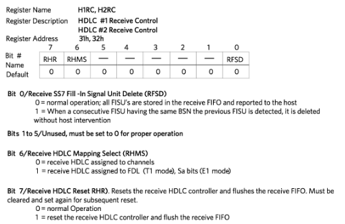
| 31 | H1RC | HDLC #1 Receive Control |
| 32 | H2RC | HDLC #2 Receive Control |
| 41 | ERCNT | Error Count Configuration Register |
| 42 | LCVCR1 | Line Code Violation Count Register 1 |
| 43 | LCVCR2 | Line Code Violation Count Register 2 |
| 44 | PCVCR1 | Path Code Violation Count Register 1 |
| 45 | PCVCR2 | Path Code Violation Count Register 2 |
| 46 | FOSCR1 | Frames Out-of-Sync Count Register 1 |
| 47 | FOSCR2 | Frames Out-of-Sync Count Register 2 |
| 48 | EBCR1 | E-Bit Count Register 1 |
| 49 | EBCR2 | E-Bit Count Register 2 |
| 4B | PCLR1 | Per-Channel Loopback Enable Register 1 |
| 4C | PCLR2 | Per-Channel Loopback Enable Register 2 |
| 4D | PCLR3 | Per-Channel Loopback Enable Register 3 |
| 4E | PCLR4 | Per-Channel Loopback Enable Register 4 |
| 4F | ESCR | Elastic Store Control Register |
| 50 | TS1 | Transmit Signaling Register 1 |
| 51 | TS2 | Transmit Signaling Register 2 |
| 52 | TS3 | Transmit Signaling Register 3 |
| 53 | TS4 | Transmit Signaling Register 4 |
| 54 | TS5 | Transmit Signaling Register 5 |
| 55 | TS6 | Transmit Signaling Register 6 |
| 56 | TS7 | Transmit Signaling Register 7 |
| 57 | TS8 | Transmit Signaling Register 8 |
| 58 | TS9 | Transmit Signaling Register 9 |
| 59 | TS10 | Transmit Signaling Register 10 |
| 5A | TS11 | Transmit Signaling Register 11 |
| 5B | TS12 | Transmit Signaling Register 12 |
| 5C | TS13 | Transmit Signaling Register 13 |
| 5D | TS14 | Transmit Signaling Register 14 |
| 5E | TS15 | Transmit Signaling Register 15 |
| 5F | TS16 | Transmit Signaling Register 16 |
| 60 | RS1 | Receive Signaling Register 1 |
| 61 | RS2 | Receive Signaling Register 2 |
| 62 | RS3 | Receive Signaling Register 3 |
| 63 | RS4 | Receive Signaling Register 4 |
| 64 | RS5 | Receive Signaling Register 5 |
| 65 | RS6 | Receive Signaling Register 6 |
| 66 | RS7 | Receive Signaling Register 7 |
| 67 | RS8 | Receive Signaling Register 8 |
| 68 | RS9 | Receive Signaling Register 9 |
| 69 | RS10 | Receive Signaling Register 10 |
| 6A | RS11 | Receive Signaling Register 11 |
| 6B | RS12 | Receive Signaling Register 12 |
| 6C | RS13 | Receive Signaling Register 13 |
| 6D | RS14 | Receive Signaling Register 14 |
| 6E | RS15 | Receive Signaling Register 15 |
| 6F | RS16 | Receive Signaling Register 16 |
| 70 | CCR1 | Common Control Register 1 |
| 71 | CCR2 | Common Control Register 2 |
| 72 | CCR3 | Common Control Register 3 |
| 73 | CCR4 | Common Control Register 4 |
| 74 | TDS0SEL | Transmit Channel Monitor Select |
| 75 | TDS0M | Transmit DS0 Monitor Register |
| 76 | RDS0SEL | Receive Channel Monitor Select |
| 77 | RDS0M | Receive DS0 Monitor Register |
| 7E | IAAR | Idle Array Address Register |
| 7F | PCICR | Per-Channel Idle Code Value Register |
| 80 | TCICE1 | Transmit Idle Code Enable Register 1 |
| 81 | TCICE2 | Transmit Idle Code Enable Register 2 |
| 82 | TCICE3 | Transmit Idle Code Enable Register 3 |
| 83 | TCICE4 | Transmit Idle Code Enable Register 4 |
| 84 | RCICE1 | Receive Idle Code Enable Register 1 |
| 85 | RCICE2 | Receive Idle Code Enable Register 2 |
| 86 | RCICE3 | Receive Idle Code Enable Register 3 |
| 87 | RCICE4 | Receive Idle Code Enable Register 4 |
| 88 | RCBR1 | Receive Channel Blocking Register 1 |
| 89 | RCBR2 | Receive Channel Blocking Register 2 |
| 8A | RCBR3 | Receive Channel Blocking Register 3 |
| 8B | RCBR4 | Receive Channel Blocking Register 4 |
| 8C | TCBR1 | Transmit Channel Blocking Register 1 |
| 8D | TCBR2 | Transmit Channel Blocking Register 2 |
| 8E | TCBR3 | Transmit Channel Blocking Register 3 |
| 8F | TCBR4 | Transmit Channel Blocking Register 4 |
| 90 | H1TC | HDLC #1 Transmit Control |
| 91 | H1FC | HDLC #1 FIFO Control |
| 92 | H1RCS1 | HDLC #1 Receive Channel Select 1 |
| 93 | H1RCS2 | HDLC #1 Receive Channel Select 2 |
| 94 | H1RCS3 | HDLC #1 Receive Channel Select 3 |
| 95 | H1RCS4 | HDLC #1 Receive Channel Select 4 |
| 96 | H1RTSBS | HDLC #1 Receive Time Slot Bits/Sa Bits Select |
| 97 | H1TCS1 | HDLC #1 Transmit Channel Select1 |
| 98 | H1TCS2 | HDLC #1 Transmit Channel Select2 |
| 99 | H1TCS3 | HDLC #1 Transmit Channel Select3 |
| 9A | H1TCS4 | HDLC #1 Transmit Channel Select4 |
| 9B | H1TTSBS | HDLC #1 Transmit Time Slot Bits/Sa Bits Select |
| 9C | H1RPBA | HDLC #1 Receive Packet Bytes Available |
| 9D | H1TF | HDLC #1 Transmit FIFO |
| 9E | H1RF | HDLC #1 Receive FIFO |
| 9F | H1TFBA | HDLC #1 Transmit FIFO Buffer Available |
| A0 | H2TC | HDLC #2 Transmit Control |
| A1 | H2FC | HDLC #2 FIFO Control |
| A2 | H2RCS1 | HDLC #2 Receive Channel Select 1 |
| A3 | H2RCS2 | HDLC #2 Receive Channel Select 2 |
| A4 | H2RCS3 | HDLC #2 Receive Channel Select 3 |
| A5 | H2RCS4 | HDLC #2 Receive Channel Select 4 |
| A6 | H2RTSBS | HDLC #2 Receive Time Slot Bits/Sa Bits Select |
| A7 | H2TCS1 | HDLC #2 Transmit Channel Select1 |
| A8 | H2TCS2 | HDLC #2 Transmit Channel Select2 |
| A9 | H2TCS3 | HDLC #2 Transmit Channel Select3 |
| AA | H2TCS4 | HDLC #2 Transmit Channel Select4 |
| AB | H2TTSBS | HDLC #2 Transmit Time Slot Bits/Sa Bits Select |
| AC | H2RPBA | HDLC #2 Receive Packet Bytes Available |
| AD | H2TF | HDLC #2 Transmit FIFO |
| AE | H2RF | HDLC #2 Receive FIFO |
| AF | H2TFBA | HDLC #2 Transmit FIFO Buffer Available |
| B0 | ESIBCR1 | Extend System Information Bus Control Register 1 |
| B1 | ESIBCR2 | Extend System Information Bus Control Register 2 |
| B2 | ESIB1 | Extend System Information Bus Register 1 |
| B3 | ESIB2 | Extend System Information Bus Register 2 |
| B4 | ESIB3 | Extend System Information Bus Register 3 |
| B5 | ESIB4 | Extend System Information Bus Register 4 |
| B6 | IBCC | In-Band Code Control Register |
| B7 | TCD1 | Transmit Code Definition Register 1 |
| B8 | TCD2 | Transmit Code Definition Register 2 |
| B9 | RUPCD1 | Receive Up Code Definition Register 1 |
| BA | RUPCD2 | Receive Up Code Definition Register 2 |
| BB | RDNCD1 | Receive Down Code Definition Register 1 |
| BC | RDNCD2 | Receive Down Code Definition Register 2 |
| BD | RSCC | In-Band Receive Spare Control Register |
| BE | RSCD1 | Receive Spare Code Definition Register 1 |
| BF | RSCD2 | Receive Spare Code Definition Register 2 |
| C5 | IBOC | Interleave Bus Operation Control Register |
| DB | BAWC | BERT Alternating Word Count Rate |
| DC | BRP1 | BERT Repetitive Pattern Set Register 1 |
| DD | BRP2 | BERT Repetitive Pattern Set Register 2 |
| DE | BRP3 | BERT Repetitive Pattern Set Register 3 |
| DF | BRP4 | BERT Repetitive Pattern Set Register 4 |
| E0 | BC1 | BERT Control Register 1 |
| E1 | BC2 | BERT Control Register 2 |
| E3 | BBC1 | BERT Bit Count Register 1 |
| E4 | BBC2 | BERT Bit Count Register 2 |
| E5 | BBC3 | BERT Bit Count Register 3 |
| E6 | BBC4 | BERT Bit Count Register 4 |
| E7 | BEC1 | BERT Error Count Register 1 |
| E8 | BEC2 | BERT Error Count Register 2 |
| E9 | BEC3 | BERT Error Count Register 3 |
| EA | BIC | BERT Interface Control Register |
| EB | ERC | Error Rate Control Register |
| EC | NOE1 | Number-of-Errors 1 |
| ED | NOE2 | Number-of-Errors 2 |
| EE | NOEL1 | Number-of-Errors Left 1 |
| EF | NOEL2 | Number-of-Errors Left 2 |
Conclusion
For further questions concerning migrating software from the DS2155 to the DS26502, please contact the Dallas Semiconductor Telecommunications applications support team via email at telecom.support@dalsemi.com or call 972-371-6555.Datasheets for the DS2155 and the DS26502 are available online at www.maxim-ic.com/telecom/
 電子發燒友App









評論