Abstract: Dallas Semiconductor/Maxim offers a variety of serial real-time clocks (RTCs). Several of these RTCs use the industry-standard Motorola SPI interface to communicate with a microprocessor. This application note helps customers understand the basics of the SPI interface.
Industry has two common formats to define the four SPI modes. The first format defines the four possible combinations of phase and polarity as mode 0, mode 1, mode 2, and mode 3. The second format defines the combinations as mode 0,0, mode 0,1, mode 1,0, and mode 1,1. The SPI master must use a mode supported by the slave device to allow proper communications.
Dallas Semiconductor/Maxim's SPI-interface RTCs support both SCLK polarities. The RTC automatically determines the polarity by detecting the idle state of SCLK when CE is asserted. The master must, therefore, place SCLK in the proper idle state before CE is asserted. Only one phase is supported. Since two SCLK polarities are supported, two of the four SPI modes are supported by the RTCs: modes 1 and 3 (mode 0,1 and mode 1,1).
On microcontrollers with built-in SPI interfaces, an SPI control or configuration register will have bits that control the polarity and phase. Because the RTC supports either polarity, the polarity can be set as desired. The phase bit, however, must be set properly, or the RTC will not operate correctly.
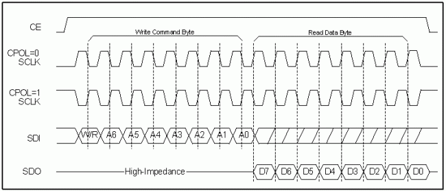
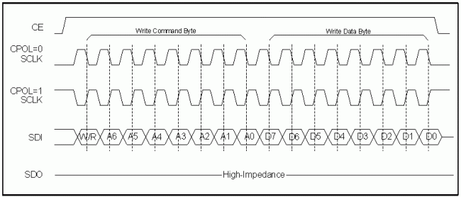
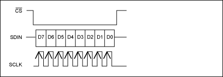
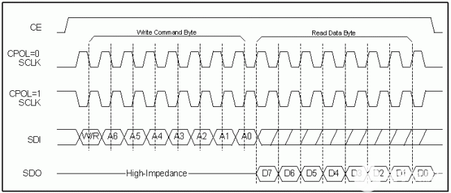
Figure 1 shows a typical single-byte read and Figure 2 shows a typical single-byte write. Each time CE is asserted, the first eight SCLK pulses are used to clock in a command byte. The command byte consists of several bits that define a register address, and one bit that defines the data direction: a write if the next eight SCLK pulses will clock data into the part, or a read if data is clocked out of the part. Additional groups of eight SCLK pulses continue to transfer data in the selected direction until CE is deasserted.
Note: In burst mode, CE is kept high and additional SCLK cycles are sent until the end of the burst.
Figure 1. Single-byte read.
Note: In burst mode, CE is kept high and additional SCLK cycles are sent until the end of the burst.
Figure 2. Single-byte write.
Examples of SPI code are available at: Real-Time Clocks
Overview
The SPI standard includes four modes, defined by the polarity of SCLK and the phase relationship between data and SCLK. The clock polarity (CPOL) is determined by the idle state of SCLK. If the idle state is low, CPOL is 0. If the idle state is high, CPOL is 1. The clock phase (CPHA) is determined by which edge that data is valid. If the data is valid on the first edge of SCLK, CPHA is 0. If the data is valid on the second edge of SCLK, CPHA is 1.Industry has two common formats to define the four SPI modes. The first format defines the four possible combinations of phase and polarity as mode 0, mode 1, mode 2, and mode 3. The second format defines the combinations as mode 0,0, mode 0,1, mode 1,0, and mode 1,1. The SPI master must use a mode supported by the slave device to allow proper communications.
Dallas Semiconductor/Maxim's SPI-interface RTCs support both SCLK polarities. The RTC automatically determines the polarity by detecting the idle state of SCLK when CE is asserted. The master must, therefore, place SCLK in the proper idle state before CE is asserted. Only one phase is supported. Since two SCLK polarities are supported, two of the four SPI modes are supported by the RTCs: modes 1 and 3 (mode 0,1 and mode 1,1).
On microcontrollers with built-in SPI interfaces, an SPI control or configuration register will have bits that control the polarity and phase. Because the RTC supports either polarity, the polarity can be set as desired. The phase bit, however, must be set properly, or the RTC will not operate correctly.
Figure 1 shows a typical single-byte read and Figure 2 shows a typical single-byte write. Each time CE is asserted, the first eight SCLK pulses are used to clock in a command byte. The command byte consists of several bits that define a register address, and one bit that defines the data direction: a write if the next eight SCLK pulses will clock data into the part, or a read if data is clocked out of the part. Additional groups of eight SCLK pulses continue to transfer data in the selected direction until CE is deasserted.

Note: In burst mode, CE is kept high and additional SCLK cycles are sent until the end of the burst.
Figure 1. Single-byte read.

Note: In burst mode, CE is kept high and additional SCLK cycles are sent until the end of the burst.
Figure 2. Single-byte write.
Examples of SPI code are available at: Real-Time Clocks
 電子發燒友App










評論